
Information


DocID022152 Rev 4 109/185
STM32F405xx, STM32F407xx Electrical characteristics
5.3.15 I/O current injection characteristics
As a general rule, current injection to the I/O pins, due to external voltage below V
SS
or
above V
DD
(for standard, 3 V-capable I/O pins) should be avoided during normal product
operation. However, in order to give an indication of the robustness of the microcontroller in
cases when abnormal injection accidentally happens, susceptibility tests are performed on a
sample basis during device characterization.
Functional susceptibilty to I/O current injection
While a simple application is executed on the device, the device is stressed by injecting
current into the I/O pins programmed in floating input mode. While current is injected into
the I/O pin, one at a time, the device is checked for functional failures.
The failure is indicated by an out of range parameter: ADC error above a certain limit (>5
LSB TUE), out of conventional limits of induced leakage current on adjacent pins (out of
5 uA/+0 uA range), or other functional failure (for example reset, oscillator frequency
deviation).
Negative induced leakage current is caused by negative injection and positive induced
leakage current by positive injection.
The test results are given in Table 46.
5.3.16 I/O port characteristics
General input/output characteristics
Unless otherwise specified, the parameters given in Table 47 are derived from tests
performed under the conditions summarized in Table 14. All I/Os are CMOS and TTL
compliant.
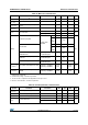
Table 45. Electrical sensitivities
Symbol Parameter Conditions Class
LU Static latch-up class T
A
= +105 °C conforming to JESD78A II level A
Table 46. I/O current injection susceptibility
Symbol Description
Functional susceptibility
Unit
Negative
injection
Positive
injection
I
INJ
(1)
1. It is recommended to add a Schottky diode (pin to ground) to analog pins which may potentially inject
negative currents.
Injected current on all FT pins –5 +0
mA
Injected current on any other pin –5 +5