SmartFusion2 FPGA Fabric DDR Controller Configuration
SmartFusion2 FPGA Fabric DDR Controller Configuration Table of Contents Introduction . . . . . . . . . . . . . . . . . . . . . . . . . . . . . . . . . . . . . . . . . . . . . . . . . . . . . . . . . . . . . . . . . . . . . . 3 1 Fabric External Memory DDR Controller Configurator . . . . . . . . . . . . . . . . . . . . . . . . . . . . . . . . . . . . . . 4 Memory Settings . . . . . . . . . . . . . . . . . . . . . . . . . . . . . . . . . . . . . . . . . . . . . . . . . . . . . . . . . . . . . . . . . . . . .
Introduction The SmartFusion2 FPGA has two embedded DDR controllers - one accessible via the MSS (MDDR) and the other intended for direct access from the FPGA Fabric (FDDR). The MDDR and FDDR both control off-chip DDR memories. To fully configure the Fabric DDR controller you must: 1. Use the Fabric External Memory DDR Controller Configurator to configure the DDR Controller, select its datapath bus interface (AXI or AHBLite), and select the DDR clock frequency as well as the fabric datapath clock frequency.
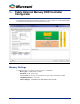
1 – Fabric External Memory DDR Controller Configurator The Fabric External Memory DDR (FDDR) Configurator is used to configure the overall datapath and the external DDR memory parameters for the Fabric DDR Controller. Figure 1-1 • FDDR Configurator Overview Memory Settings Use Memory Settings to configure your memory options in the MDDR.
Fabric Interface Settings FPGA Fabric Interface - This is the data interface between the FDDR and the FPGA design. Because the FDDR is a memory controller, it is intended to be a slave on an AXI or AHB bus. The Master of the bus initiates bus transactions, which are in turn interpreted by the FDDR as memory transactions and communicated to the off-chip DDR Memory. FDDR fabric interface options are: • Using an AXI-64 Interface - One master accesses the FDDR through a 64-bit AXI interface.
Enable Interrupts The FDDR is capable of raising interrupts when certain predefined conditions are satisfied. Check Enable Interrupts in the FDDR configurator if you would like to use these interrupts in your application. This exposes the interrupt signals on the FDDR instance. You can connect these interrupt signals as your design requires.
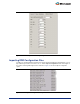
2 – FDDR Controller Configuration When you use the Fabric DDR Controller to access an external DDR Memory, the DDR Controller must be configured at runtime. This is done by writing configuration data to dedicated DDR controller configuration registers. This configuration data is dependent on the characteristics of the external DDR memory and your application.
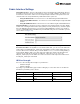
Figure 2-1 • FDDR Configuration - Memory Initialization Tab 8
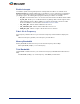
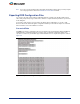
Figure 2-2 • FDDR Configuration - Memory Timing Tab Importing DDR Configuration Files In addition to entering DDR Memory parameters using the Memory Initialization and Timing tabs, you can import DDR register values from a file. To do so, click the Import Configuration button and navigate to the text file containing DDR register names and values. Figure 2-3 shows the import configuration syntax.
Note: If you choose to import register values rather than entering them using the GUI, you must specify all necessary register values. Refer to the SmartFusion2 User Guide for details. Exporting DDR Configuration Files You can also export the current register configuration data into a text file. This file will contain register values that you imported (if any) as well as those that were computed from GUI parameters you entered in this dialog box.
Firmware When you generate the SmartDesign, the following files are generated in the /firmware/ drivers_config/sys_config directory. These files are required for the CMSIS firmware core to compile properly and contain information regarding your current design, including peripheral configuration data and clock configuration information for the MSS. Do not edit these files manually, as they are recreated every time your root design is regenerated. • sys_config.c • sys_config.
Note: If you are using System Builder the configuration path is set and connected automatically. Figure 2-5 • FIC_2 Configurator Overview To configure the FIC_2 interface: 1. Open the FIC_2 configurator dialog (Figure 2-5) from the MSS configurator. 2. Select the Initialize peripherals using Cortex-M3 option. 3. Make sure that the MSS DDR is checked, as are the Fabric DDR/SERDES blocks if you are using them. 4. Click OK to save your settings.
3 – Port Description FDDR Core Ports Table 3-1 • FDDR Core Ports Port Name Direction Description CORE_RESET_N IN FDDR Controller Reset CLK_BASE IN FDDR Fabric Interface Clock FPLL_LOCK OUT FDDR PLL Lock output - high when FDDR PLL is locked CLK_BASE_PLL_LOCK IN Fabric PLL Lock Input. This input is exposed only when the Use FAB_PLL_LOCK option is selected. Interrupt Ports This group of ports is exposed when you select the Enable Interrupts option.
DDR PHY Interface Table 3-4 • DDR PHY Interface Port Name Direction Description FDDR_CAS_N OUT DRAM CASN FDDR_CKE OUT DRAM CKE FDDR_CLK OUT Clock, P side FDDR_CLK_N OUT Clock, N side FDDR_CS_N OUT DRAM CSN FDDR_ODT OUT DRAM ODT FDDR_RAS_N OUT DRAM RASN FDDR_RESET_N OUT DRAM Reset for DDR3 FDDR_WE_N OUT DRAM WEN FDDR_ADDR[15:0] OUT Dram Address bits FDDR_BA[2:0] OUT Dram Bank Address FDDR_DM_RDQS[4:0] INOUT Dram Data Mask FDDR_DQS[4:0] INOUT Dram Data Strobe Input/Out
AXI Bus Interface Table 3-5 • AXI Bus Interface Port Name Direction Description AXI_S_AWREADY OUT Write address ready AXI_S_WREADY OUT Write address ready AXI_S_BID[3:0] OUT Response ID AXI_S_BRESP[1:0] OUT Write response AXI_S_BVALID OUT Write response valid AXI_S_ARREADY OUT Read address ready AXI_S_RID[3:0] OUT Read ID Tag AXI_S_RRESP[1:0] OUT Read Response AXI_S_RDATA[63:0] OUT Read data AXI_S_RLAST OUT Read Last - This signal indicates the last transfer in a read burst.
Table 3-5 • AXI Bus Interface (continued) Port Name Direction Description AXI_S_CORE_RESET_N IN MDDR Global Reset AXI_S_RMW IN Indicates whether all bytes of a 64-bit lane are valid for all beats of an AXI transfer. 0: Indicates that all bytes in all beats are valid in the burst and the controller should default to write commands. 1: Indicates that some bytes are invalid and the controller should default to RMW commands.
AHB0 Bus Interface Table 3-6 • AHB0 Bus Interface Port Name Direction Description AHB0_S_HREADYOUT OUT AHBL slave ready - When high for a write indicates the slave is ready to accept data and when high for a read indicates that data is valid. AHB0_S_HRESP OUT AHBL response status - When driven high at the end of a transaction indicates that the transaction has completed with errors. When driven low at the end of a transaction indicates that the transaction has completed successfully.
AHB1 Bus Interface Table 3-7 • AHB1 Bus Interface Port Name Direction Description AHB1_S_HREADYOUT OUT AHBL slave ready - When high for a write, indicates the slave is ready to accept data, and when high for a read, indicates that data is valid. AHB1_S_HRESP OUT AHBL response status - When driven high at the end of a transaction indicates that the transaction has completed with errors. When driven low at the end of a transaction, indicates that the transaction has completed successfully.
A – Product Support Microsemi SoC Products Group backs its products with various support services, including Customer Service, Customer Technical Support Center, a website, electronic mail, and worldwide sales offices. This appendix contains information about contacting Microsemi SoC Products Group and using these support services. Customer Service Contact Customer Service for non-technical product support, such as product pricing, product upgrades, update information, order status, and authorization.
My Cases Microsemi SoC Products Group customers may submit and track technical cases online by going to My Cases. Outside the U.S. Customers needing assistance outside the US time zones can either contact technical support via email (soc_tech@microsemi.com) or contact a local sales office. Sales office listings can be found at www.microsemi.com/soc/company/contact/default.aspx.