
User Guide

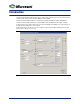

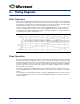


Table Of Contents

7
3 – Timing Diagrams
Write Operation
During a write operation when the WE signal is asserted the FIFO stores the value on the DATA bus into
the memory. The WACK signal is asserted each time a successful write operation occurs on the FIFO. If
the FIFO fills up, the FULL flag is asserted indicating that no more data can be written. The AFULL flag is
asserted when the number of elements in the FIFO equals the threshold amount.
If a write operation is attempted while the FIFO is full, the OVERFLOW signal is asserted on the next
clock cycle, indicating that an error has occurred. The OVERFLOW signal is asserted for each write
operation that fails. A sample timing diagram of a FIFO with depth configuration of 4, almost full value set
to 3, and rising clock edge is shown in
Figure 3-1.
Read Operation
During a read operation when the RE signal is asserted the FIFO reads a data value onto the Q bus from
the memory. The data is available to the client two clock cycles after the assertion of the RE, this data is
held on the bus until the next RE is asserted. The DVLD signal is asserted on the same clock cycle that
the data is available. Therefore, the client logic can monitor the DVLD signal for indication of valid data.
However, DVLD only asserts for the first clock cycle that the new data is available, whereas the actual
data may still be on the data bus.
If the FIFO is emptied then the EMPTY flag is asserted to indicate that no more data elements can be
read. The AEMPTY flag is asserted when the number of elements in the FIFO equals the set threshold
amount.
If a read operation is attempted while the FIFO is empty, the UNDERFLOW signal is asserted on the next
clock cycle indicating that an error has occurred. The UNDERFLOW signal is asserted for each read
operation that fails.
Figure 3-1 • Write Operation and Flags