
User Guide
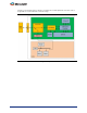
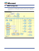
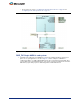
Table Of Contents
- Introduction
- 1 – MSS Configurator
- 2 – SmartDesign and MSS Configurator Actions
- 3 – Configuring the DDR_FIC Sub-System
- 4 – Configuring the SMC_FIC Sub-System
- 5 – Configuring the FIC Sub-Systems
- 6 – Configuring the FIC Sub-System Clocks
- 7 – Configuring the FIC Sub-System Reset
- 8 – Configuring the System Memory Map
- A – Product Support

5
The MSS contains:
1. AHB_Bus matrix; all transactions in the MSS go through this block.
2. DDR Controller -interfaces with the DDR_FIC.
3. DDR_FIC (SMC_FIC) sub-block (used if you enable the FPGA fabric to DDR path in the
MSS_MDDR configurator).
4. FIC_0 sub-block.
5. FIC_1 sub-block (in larger devices only).
6. FIC_2 sub-block (for APB initialization of SERDES and external DDRs).
7. MSS_CCC sub-block needed to configure the FIC clocks relative to the MSS main clock
(M3_CLK).
8. MSS_RESET sub-block that generates the MSS internal resets as well as the
MSS_RESET_N_M2F signal that drives the FPGA fabric.
The FPGA fabric contains:
1. Three FIC sub-systems (DDR_FIC, FIC_0 and FIC_1).
2. Fabric CCC - FAB_CCC - required to generate the clocks that drive the FPGA fabric FIC sub-
system as well as the MCCC_CLK_BASE port on the MSS block.
3. FAB_CCC reference clock signal - can be one of the on-chip oscillators, an external crystal
oscillator, a clock generated internally to the fabric or from outside the chip.
The block diagram also shows the clock network in red and the reset network in dark blue.
This document discusses each of these blocks and describes how to connect the clocks and resets.
Figure 2 • MSS to FPGA Fabric Block Diagram - SMC_FIC Mode