
User Guide
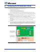
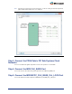


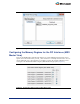
Table Of Contents
- Introduction
- 1 – MSS Configurator
- 2 – SmartDesign and MSS Configurator Actions
- 3 – Configuring the DDR_FIC Sub-System
- 4 – Configuring the SMC_FIC Sub-System
- 5 – Configuring the FIC Sub-Systems
- 6 – Configuring the FIC Sub-System Clocks
- 7 – Configuring the FIC Sub-System Reset
- 8 – Configuring the System Memory Map
- A – Product Support

24
Step 1: Configure the MSS CCC Sub-Block
For each FIC block (FIC_0, FIC_1, and DDR_FIC/SMC_FIC) used in your design, select the clock
divisors in the MSS Clock Configurator (MSS_CCC) as shown in
Figure 6-2.
Note that the CLK_BASE field is non-editable. The CLK_BASE frequency, as imposed by the
SmartFusion2 architecture, must be the minimum frequency of all FIC clock frequencies and is
automatically computed by the MSS CCC configurator. See
"Step 3: Connect the FPGA Fabric FIC Sub-
Systems Clock Networks" on page 25
for more details about CLK_BASE configuration.
Step 2: Configure the FPGA Fabric FIC clocks
Instantiate a fabric CCC (with PLL) and configure it to satisfy the FIC sub-system clock rules described
on page
23. You typically need to associate a global output (GLx) for each of the FIC clocks, specify for
each output its frequency (matching the frequencies defined in the MSS CCC) and have all global
outputs derived from the output of the PLL to guarantee the phase alignment (as shown in
Figure 6-3).
Figure 6-2 • MSS CCC FIC Clock Configuration