SmartFusion2 MSS Creating a Design Using MSS Fabric Interfaces
SmartFusion2 MSS Creating a Design Using MSS Fabric Interfaces Table of Contents Introduction . . . . . . . . . . . . . . . . . . . . . . . . . . . . . . . . . . . . . . . . . . . . . . . . . . . . . . . . . . . . . . . . . . . . . . 3 High-Level View . . . . . . . . . . . . . . . . . . . . . . . . . . . . . . . . . . . . . . . . . . . . . . . . . . . . . . . . . . . . . . . . . . . . . . . . . . . . 3 1 MSS Configurator. . . . . . . . . . . . . . . . . . . . . . . . . . . . . . . . . . . . . . . . . . .
Introduction The SmartFusion2 Microcontroller Sub-System (MSS) offers four different Fabric Interface Controllers (FIC): • DDR_FIC • SMC_FIC • FIC_0 and FIC_1, depending on your device These interface blocks enable the MSS to interface with logic implemented in the FPGA fabric and vice versa. The DDR_FIC is used when you configure the MSS DDR block (MDDR) such that the external DDR memory can be accessed from an FPGA fabric master via an AXI interface or 2 AHBLite AMBA interfaces.
interfaces in your design. However, this does not change the overall requirements for how to create a design with one or more FIC block used in the design.
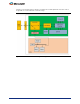
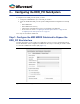
Figure 2 • MSS to FPGA Fabric Block Diagram - SMC_FIC Mode The MSS contains: 1. AHB_Bus matrix; all transactions in the MSS go through this block. 2. DDR Controller -interfaces with the DDR_FIC. 3. DDR_FIC (SMC_FIC) sub-block (used if you enable the FPGA fabric to DDR path in the MSS_MDDR configurator). 4. FIC_0 sub-block. 5. FIC_1 sub-block (in larger devices only). 6. FIC_2 sub-block (for APB initialization of SERDES and external DDRs). 7.
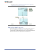
1 – MSS Configurator This document refers to certain MSS sub-blocks that must be configured as part of creating a design where the MSS interfaces to the FPGA fabric via the FIC sub-blocks. Those blocks are highlighted in red in Figure 1-1.
2 – SmartDesign and MSS Configurator Actions There are several common actions referenced in this document; they are summarized in the following list:. If you are familiar with SmartDesign and the MSS you can skip to the next section. Instantiating a core - The action of selecting a core from the Libero SoC IP catalog, dragging and dropping that core onto a SmartDesign Canvas.
3 – Configuring the DDR_FIC Sub-System To configure/create a DDR_FIC sub-system, you must: 1. Configure the MSS MDDR to expose the DDR_FIC interface 2.
Step 2: Create the FPGA Fabric DDR_FIC Sub-System Based on the FPGA bus connection type you selected - AXI, Single AHBLite or Two AHBLite - you must create a sub-system that matches your selection. DDR_FIC/AXI Sub-System 1. Instantiate and configure the CoreAXI IP core from the Catalog window. Enable the slots you plan to use for your application as well as the amount of memory per slot that matches your design requirements.
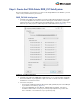
– Clocks and resets; refer to "Configuring the FIC Sub-System Clocks" on page 23 and "Configuring the FIC Sub-System Reset" on page 27. Figure 3-3 • DDR_FIC AXI Sub-System DDR_FIC/Single-AHBLite sub-system 1. Instantiate and configure the CoreAHBLite IP core from the Catalog. Enable the slots that you plan to use for your application as shown in Figure 3-4. In this example, CoreAHBLite is configured to address one 4GB of DDR RAM memory space using slot0 from master M0.
Figure 3-4 • Core AHBLite - Combined Region Master Configuration 2. Instantiate and configure the AMBA AHBLite compliant master core or component that is intended to master to the CoreAHBLite bus. If your application requires more than one master onto the CoreAHBLite bus, instantiate the additional masters too. Up to four masters are supported on the CoreAHBLite bus. 3.
– Clocks and resets; refer to "Configuring the FIC Sub-System Clocks" on page 23 and "Configuring the FIC Sub-System Reset" on page 27. Figure 3-5 • DDR_FIC AHBLite Sub-System DDR_FIC/Two AHBLite Sub-System When you select the two AHBLite Interfaces option for the MDDR, an additional BIF, MDDR_DDR_AHB1_SLAVE BIF, is exposed at the MSS component for you to connect to the new slave.
4 – Configuring the SMC_FIC Sub-System Although the SMC_FIC can be used as an AXI or AHBLite bus interface, this document only describes how to use the SMC_FIC interface configured in AXI mode to connect to the CoreSDR_AXI core. That core is an AXI-based SDR RAM controller used to connect, in this case, the MSS to an external Single Data Rate (SDR) memory component. You can easily infer how to use the AHBLite interface from the following description; the steps are very similar.
(Right-click the MSS Component and choose Update Instances with Latest Component). The MDDR_SMC_AXI_MASTER is exposed as a Bus Interface Port of the MSS component.
Step 2: Create the FPGA Fabric SMC_FIC Sub-System 1. Instantiate and configure the CoreAXI such that the master slot M0 is enabled for the slave slot S0, as shown in Figure 4-2. Since you are addressing an external memory via a soft memory controller, your slot size selection should match the amount of external memory space that you plan on addressing from the Cortex-M3 processor or any master writing to that external memory via the MSS DDR bridge. Figure 4-2 • CoreAXI Configuration - SMC_FIC Mode 2.
– Clocks and resets; refer to "Configuring the FIC Sub-System Clocks" on page 23 and "Configuring the FIC Sub-System Reset" on page 27.
5 – Configuring the FIC Sub-Systems To configure/create a FIC sub-system, you must: 1. Configure the MSS FIC to expose the FIC interface 2.
Step 2: Create the FPGA Fabric FIC Sub-System For each FIC interface exposed - master and slave, you must instantiate a bus (CoreAHBLite or CoreAPB3) that matches the type you selected. Depending on the interface role (master/slave) and type (AHBLite/APB3), the bus must be configured as follows: Master/AHBLite Instantiate and configure the CoreAHBLite bus as follows: 1.
Figure 5-5 • Master/AHBLite Master Access Configuration 3. Instantiate and configure AHBLite compliant peripheral cores and/or custom AHBLite compliant components. 4. Connect the sub-system: – Connect the CoreAHBLite mirrored-master Bus Interface (BIF) port M1 to the MSS master BIF port - FIC_0/1_AHB_MASTER - as shown in Figure 5-6. – Connect the AHBLite slaves to the proper slots as per your memory map requirement.
– Clocks and resets; refer to "Configuring the FIC Sub-System Clocks" on page 23 and "Configuring the FIC Sub-System Reset" on page 27.
Master/APB3 Instantiate and configure the CoreAPB3 bus as follows: 1. Select the Address Configuration options as shown in Figure 5-7. This mode provides sixteen 16MB slots that can be used to connect up to sixteen APB3 compliant slaves. If you need slots with more memory, you can combine multiple slaves to build a larger slot. Refer to the CoreAPB3 User’s Guide for more details about this option. Figure 5-7 • Master/APB3 Address Configuration 2.
– Clocks and resets; refer to "Configuring the FIC Sub-System Clocks" on page 23 and "Configuring the FIC Sub-System Reset" on page 27. Figure 5-9 • FIC Master/APB3 Sub-System Slave/AHBLite Not available at this time. Slave/APB3 Not available at this time.
6 – Configuring the FIC Sub-System Clocks To create the proper clock configuration and connectivity, you must: • Configure the MSS CCC FIC clocks • Instantiate and configure an FPGA fabric CCC core • Connect the clock networks for each FIC sub-system • Connect the MSS CLK_BASE port to the correct FPGA fabric FIC sub-system clock network The SmartFusion2 architecture imposes a number of rules that must be followed for all FIC sub-systems to interact properly between the MSS logic and FPGA fabric logi
Step 1: Configure the MSS CCC Sub-Block For each FIC block (FIC_0, FIC_1, and DDR_FIC/SMC_FIC) used in your design, select the clock divisors in the MSS Clock Configurator (MSS_CCC) as shown in Figure 6-2. Figure 6-2 • MSS CCC FIC Clock Configuration Note that the CLK_BASE field is non-editable. The CLK_BASE frequency, as imposed by the SmartFusion2 architecture, must be the minimum frequency of all FIC clock frequencies and is automatically computed by the MSS CCC configurator.
Note: If two FIC sub-systems have the same frequencies, you do not need to generate two independent global outputs from the fabric CCC; one is sufficient. Figure 6-3 • Fabric CCC with PLL Step 3: Connect the FPGA Fabric FIC Sub-Systems Clock Networks Connect each fabric CCC global output GLx to the FIC sub-system it is associated with. Step 4: Connect the MSS CLK_BASE Port Connect the slowest of the fabric CCC global output GLx to the MSS CLK_BASE port.
Timing Analysis Requirements Perform post-layout static timing analysis to make sure that the design meets the timing requirements defined in the MSS CCC and FPGA fabric CCC Configurators. You may have to change M3_CLK or increase the clock ratio between the MSS and the fabric to get a design that passes Static Timing Analysis.
7 – Configuring the FIC Sub-System Reset To configure the FIC Sub-System Reset: 1. From the MSS Configurator, configure the MSS Reset sub-block to expose the MSS_RESET_N_M2F port. Figure 7-1 • Configure the MSS Reset Sub-Block 2. Connect the MSS_RESET_N_M2F port to all FPGA fabric FIC sub-systems reset ports.
8 – Configuring the System Memory Map Each peripheral (AMBA AXI, AHBLite and APB3 slaves) is identified by an address from the FIC subsystem's master point of view. We usually refer to the overall relationships between masters and slaves of a sub-system as the memory map of that sub-system. The memory map of a sub-system can be edited in SmartDesign. You can also view the final memory map of your system when you generate the entire system.
Figure 8-2 • Modify Memory Map Dialog Box Configuring the Memory Regions for the FIC Interfaces (MSS Master View) There are six 256 MB regions defined as FIC Regions 0 to 5 in the MSS memory map. Each of these regions can be allocated to the FIC_0 or FIC_1 slave interfaces in a mutually exclusive fashion. You can select to which FIC (0 or 1) slave interface you assign those regions by using the radio button next to each region in the FPGA Fabric Address Regions (MSS Master View) group box (Figure 8-3).
Memory Map Computation General Formula The possible base addresses for the FIC fabric interfaces are 0x30000000, 0x50000000, 0x70000000, 0x80000000, 0x90000000 and 0xF0000000. See "Configuring the FIC Sub-Systems" on page 17 for details on how to configure each FIC instance to map to these addresses. For AHBLite, the slot size can either be 16 MB (0x01000000) or 256 MB (0x10000000).
A – Product Support Microsemi SoC Products Group backs its products with various support services, including Customer Service, Customer Technical Support Center, a website, electronic mail, and worldwide sales offices. This appendix contains information about contacting Microsemi SoC Products Group and using these support services. Customer Service Contact Customer Service for non-technical product support, such as product pricing, product upgrades, update information, order status, and authorization.
My Cases Microsemi SoC Products Group customers may submit and track technical cases online by going to My Cases. Outside the U.S. Customers needing assistance outside the US time zones can either contact technical support via email (soc_tech@microsemi.com) or contact a local sales office. Sales office listings can be found at www.microsemi.com/soc/company/contact/default.aspx.