
Operating Manual


HP900 Operating Manual 7
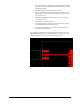
• The transmission lines width and spacing to GND must be uniform
and routed as smoothly as possible: avoid abrupt changes of width
and spacing to GND
• Add GND stitching vias around transmission lines
• Ensure solid metal connection of the adjacent metal layer on the
PCB stack-up to main ground layer, providing enough vias on the
adjacent metal layer
• Route RF transmission lines far from any noise source and from
any sensitive circuits
• Avoid stubs on the transmission lines
• Avoid signal routing in parallel to transmission lines or crossing
the transmission lines on buried metal layer
• Do not route microstrip lines below discrete component or other
mechanics placed on top layer
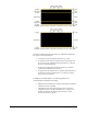
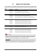
An example of proper RF circuit design is shown below. In this case, the
RF_Antenna pin is directly connected to SMA connectors by means of a
50Ω transmission line, with the recommended design layout.