
Operating Manual


6 HP900 Operating Manual
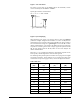
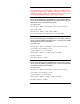
Example of 50 Ω coplanar waveguide transmission line for 4-layer PCB
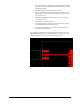
Example of 50 Ω coplanar waveguide transmission line for 2-layer PCB
To achieve a 50Ω characteristic impedance, the width of the transmission
line must be chosen depending on:
• the thickness of the transmission line itself (e.g. 35 μm)
• the thickness of the dielectric material between the top layer and
the next inner layer implementing the ground plane (e.g. 270 μm
(4-Layer), 1510 μm(2-Layer))
• the dielectric constant of the dielectric material (e.g. dielectric
constant of the FR-4 dielectric material)
• the gap from the transmission line to the adjacent ground plane on
the same layer of the transmission line (e.g. 500 μm in 4 Layer,
400 μm in 2 Layer boards).
In Addition to the 50Ω impedance, the following guidelines are
recommended for transmission lines design:
• Minimize the transmission line length: the insertion loss should be
minimized as much as possible
• Add GND clearance on buried metal layers below any pad of
component present on the RF transmission lines, if top-layer to
buried layer dielectric thickness is below 200 μm, to reduce
parasitic capacitance to ground