
Datasheet

2
Supertex inc.
www.supertex.com
Doc.# DSFP-TN2510
A062113
TN2510
Electrical Characteristics (T
A
= 25
O
C unless otherwise specied)
Sym Parameter Min Typ Max Units Conditions
BV
DSS
Drain-to-source breakdown voltage 100 - - V V
GS
= 0V, I
D
= 2.0mA
V
GS(th)
Gate threshold voltage 0.6 - 2.0 V V
GS
= V
DS
, I
D
= 1.0mA
ΔV
GS(th)
Change in V
GS(th)
with temperature - - -4.5 mV/
O
C V
GS
= V
DS
, I
D
= 1.0mA
I
GSS
Gate body leakage - - 100 nA V
GS
= ± 20V, V
DS
= 0V
I
DSS
Zero gate voltage drain current
- - 10 µA V
GS
= 0V, V
DS
= Max Rating
- - 1.0 mA
V
DS
= 0.8 Max Rating,
V
GS
= 0V, T
A
= 125°C
I
D(ON)
On-state drain current
1.2 2.0 -
A
V
GS
= 5.0V, V
DS
= 25V
3.0 6.0 - V
GS
= 10V, V
DS
= 25V
R
DS(ON)
Static drain-to-source on-state resistance
- - 15
Ω
V
GS
= 3.0V, I
D
= 250mA
- 1.5 2.0 V
GS
= 4.5V, I
D
= 750mA
- 1.0 1.5 V
GS
= 10V, I
D
= 750mA
ΔR
DS(ON)
Change in R
DS(ON)
with temperature - - 0.75 %/
O
C V
GS
= 10V, I
D
= 750mA
G
FS
Forward transductance 400 800 - mmho V
DS
= 25V, I
D
= 1.0A
C
ISS
Input capacitance - 70 125
pF
V
GS
= 0V,
V
DS
= 25V,
f = 1.0MHz
C
OSS
Common source output capacitance - 30 70
C
RSS
Reverse transfer capacitance - 15 25
t
d(ON)
Turn-on delay time - - 10
ns
V
DD
= 25V,
I
D
= 1.5A,
R
GEN
= 25Ω
t
r
Rise time - - 10
t
d(OFF)
Turn-off delay time - - 20
t
f
Fall time - - 10
V
SD
Diode forward voltage drop - - 1.8 V V
GS
= 0V, I
SD
= 1.5A
t
rr
Reverse recovery time - 300 - ns V
GS
= 0V, I
SD
= 1.5A
Notes:
1. All D.C. parameters 100% tested at 25
O
C unless otherwise stated. (Pulse test: 300µs pulse, 2% duty cycle.)
2. All A.C. parameters sample tested.
Notes:
† I
D
(continuous) is limited by max rated T
j
.
‡ Mounted on FR5 Board, 25mm x 25mm x 1.57mm.
Thermal Characteristics
Package
I
D
(continuous)
†
I
D
(pulsed)
Power Dissipation
@T
A
= 25
O
C
I
DR
†
I
DRM
TO-243AA (SOT-89) 730mA 5.0A 1.6W
‡
730mA 5.0A
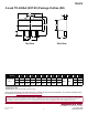
Switching Waveforms and Test Circuit
90%
10%
90%
90%
10%
10%
Pulse
Generator
VDD
R
L
OUTPUT
D.U.T.
t
(ON)
t
d(ON)
t
(OFF)
t
d(OFF)
t
r
INPUT
INPUT
OUTPUT
10V
VDD
R
GEN
0V
0V
t
f