
Datasheet


© 2011 Microchip Technology Inc. DS22049F-page 3
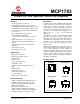
MCP1703
1.0 ELECTRICAL
CHARACTERISTICS
Absolute Maximum Ratings †
V
DD
..................................................................................+18V
All inputs and outputs w.r.t. .............(V
SS
-0.3V) to (V
IN
+0.3V)
Peak Output Current ...................................................500 mA
Storage temperature .....................................-65°C to +150°C
Maximum Junction Temperature.................................+150°C
ESD protection on all pins (HBM;MM)............... ≥ 4kV; ≥ 400V
† Notice: Stresses above those listed under “Maximum
Ratings” may cause permanent damage to the device. This is
a stress rating only and functional operation of the device at
those or any other conditions above those indicated in the
operational listings of this specification is not implied.
Exposure to maximum rating conditions for extended periods
may affect device reliability.
DC CHARACTERISTICS
Electrical Specifications: Unless otherwise specified, all limits are established for V
IN
= V
OUT(MAX)
+ V
DROPOUT(MAX)
, Note 1,
I
LOAD
= 100 µA, C
OUT
= 1 µF (X7R), C
IN
= 1 µF (X7R), T
A
= +25°C.
Boldface type applies for junction temperatures, T
J
(Note 7) of -40°C to +125°C.
Parameters Symbol Min Typ Max Units Conditions
Input / Output Characteristics
Input Operating Voltage V
IN
2.7 — 16.0 V Note 1
Input Quiescent Current I
q
—2.0 5 µA I
L
= 0 mA
Maximum Output Current I
OUT_mA
250 — — mA For V
R
≥ 2.5V
50 100 — mA For V
R
< 2.5V, V
IN
≥ 2.7V
100 130 — mA For V
R
< 2.5V, V
IN
≥ 2.95V
150 200 — mA For V
R
< 2.5V, V
IN
≥ 3.2V
200 250 — mA For V
R
< 2.5V, V
IN
≥ 3.45V
Output Short Circuit Current I
OUT_SC
— 400 — mA V
IN
= V
IN(MIN)
(Note 1), V
OUT
= GND,
Current (average current) measured
10 ms after short is applied.
Output Voltage Regulation V
OUT
V
R
-3.0% V
R
±0.4% V
R
+3.0% V Note 2
V
R
-2.0% V
R
±0.4% V
R
+2.0% V
V
R
-1.0% V
R
±0.4% V
R
+1.0% V 1% Custom
V
OUT
Temperature Coefficient TCV
OUT
— 50 — ppm/°C Note 3
Line Regulation ΔV
OUT
/
(V
OUT
XΔV
IN
)
-0.3 ±0.1 +0.3 %/V (V
OUT(MAX)
+ V
DROPOUT(MAX)
) ≤ V
IN
≤ 16V, Note 1
Load Regulation
ΔV
OUT
/V
OUT
-2.5 ±1.0 +2.5 %I
L
= 1.0 mA to 250 mA for V
R
>= 2.5V
I
L
= 1.0 mA to 200 mA for V
R
< 2.5V
V
IN
= 3.65V, Note 4
Note 1: The minimum V
IN
must meet two conditions: V
IN
≥ 2.7V and V
IN
≥ (V
OUT(MAX)
+ V
DROPOUT(MAX)
).
2: V
R
is the nominal regulator output voltage. For example: V
R
= 1.2V, 1.5V, 1.8V, 2.5V, 2.8V, 3.0V, 3.3V, 4.0V, or 5.0V.
The input voltage V
IN
= V
OUT(MAX)
+ V
DROPOUT(MAX)
or Vi
IN
= 2.7V (whichever is greater); I
OUT
= 100 µA.
3: TCV
OUT
= (V
OUT-HIGH
- V
OUT-LOW
) *10
6
/ (V
R
* ΔTemperature), V
OUT-HIGH
= highest voltage measured over the
temperature range. V
OUT-LOW
= lowest voltage measured over the temperature range.
4: Load regulation is measured at a constant junction temperature using low duty cycle pulse testing. Changes in output
voltage due to heating effects are determined using thermal regulation specification TCV
OUT
.
5: Dropout voltage is defined as the input to output differential at which the output voltage drops 2% below its measured
value with an applied input voltage of V
OUT(MAX)
+ V
DROPOUT(MAX)
or 2.7V, whichever is greater.
6: The maximum allowable power dissipation is a function of ambient temperature, the maximum allowable junction
temperature and the thermal resistance from junction to air (i.e., T
A
, T
J
, θ
JA
). Exceeding the maximum allowable power
dissipation will cause the device operating junction temperature to exceed the maximum 150°C rating. Sustained
junction temperatures above 150°C can impact the device reliability.
7: The junction temperature is approximated by soaking the device under test at an ambient temperature equal to the
desired junction temperature. The test time is small enough such that the rise in the junction temperature over the
ambient temperature is not significant.