
Datasheet


2016 Microchip Technology Inc. DS00002246A-page 15
KSZ8895MQX/RQX/FQX/MLX
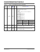
108 MDIO IPU/O All
PHYs MII management (MIIM registers) data I/O. Or SMI interface
data I/O
Note: Need an external pull-up when driven.
109 SPIQ IPU/O All
SPI serial data output in SPI slave mode.
Note: Need an external pull-up when driven.
110 SPIC/SCL IPU/O All
(1) Input clock up to 25 MHz in SPI slave mode,
(2) Output clock at 61 kHz in I
2
C master mode. See “Pin 113.”
Note: Need an external pull-up when driven.
111 SSPID/SDA IPU/O All
(1) Serial data input in SPI slave mode;
(2) Serial data input/output in I
2
C master mode. See “Pin 113.”
Note: Need an external pull-up when driven.
112 SPIS_N IPU All
Active low.
(1) SPI data transfer start in SPI slave mode. When SPIS_N is high,
the KSZ8895MQX/RQX/FQX/MLX is deselected and SPIQ is held
in high impedance state, a high-to-low transition to initiate the SPI
data transfer.
(2) not used in I
2
C master mode.
113 PS1 IPD —
Serial bus configuration pin.
For this case, if the EEPROM is not present, the KSZ8895MQX/
RQX/FQX/MLX will start itself with the PS [1:0] = 00 default register
values.
Pin Configuration Serial Bus Configuration
PS[1:0] = 00 I
2
C Master Mode for EEPROM
PS[1:0] = 01 SMI Interface Mode
PS[1:0] = 10
SPI Slave Mode for CPU
Interface
PS[1:0] = 11 Factory Test Mode (BIST)
114 PS0 IPD — Serial bus configuration pin. See “Pin 113.”
115 RST_N IPU — Reset the KSZ8895MQX/RQX/FQX/MLX device. Active low.
116 GNDD GND — Digital ground.
117 VDDC P — 1.2V digital core V
DD
.
118 TESTEN IPD — NC for normal operation. Factory test pin.
119 SCANEN IPD — NC for normal operation. Factory test pin.
120 NC NC — No connection. Leave NC pin floating.
121 X1 I —
25 MHz crystal clock connection/or 3.3V Oscillator input. Crystal/
Oscillator should be ±50 ppm tolerance.
122 X2 O — 25 MHz crystal clock connection.
TABLE 2-1: SIGNALS - KSZ8895MQX/RQX/FQX/MLX (CONTINUED)
Pin
Number
Pin
Name
Type,
Note
2-1
Port Pin Function, Note 2-2