
Datasheet


KSZ8895MQX/RQX/FQX/MLX
DS00002246A-page 14 2016 Microchip Technology Inc.
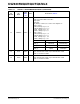
95 LED4-0 IPU/O 4
LED indicator 0.
Strap option:
PU (default) = Normal mode.
PD = Energy Detection mode (EDPD mode)
Strap to Register 14 bits [4:3]
96 LED3-2 IPU/O 3 LED indicator 2.
97 LED3-1 IPU/O 3 LED indicator 1.
98 LED3-0 IPU/O 3
LED indicator 0.
Strap option:
PU (default) = Select I/O drive strength (8 mA);
PD = Select I/O drive strength (12 mA).
Strap to Register132 bit [7-6].
99 GNDD GND — Digital ground.
100 VDDIO P — 3.3V, 2.5V, or 1.8V digital V
DD
for digital I/O circuitry.
101 LED2-2 IPU/O 2
LED indicator 2.
Strap option for RQX only:
PU (default) = Select the device as clock mode in SW5- RMII,
25MHz crystal/oscillator to X1/X2 pins of the device and pins of
SMRXC and PMRXC output 50 MHz clock.
PD = Select the device as normal mode in SW5-RMII. Switch
MAC5 used only. The input clock from X1/X2 pins is not used, the
device’s clock source comes from SMTXC/SMREFCLK pin which
the 50 MHz reference clock comes from external 50 MHz clock
source, PMRXC can output 50 MHz clock for P5-RMII interface in
the normal mode.
102 LED2-1 IPU/O 2
LED indicator 1.
Strap option: for Port 3 only.
PU (default) = Enable auto-negotiation.
PD = Disable auto-negotiation. Strap to Register60 bit [7].
103 LED2-0 IPU/O 2 LED indicator 0.
104 LED1-2 IPU/O 1 LED indicator 2.
105 LED1-1 IPU/O 1
LED indicator 1.
Strap option: for port 3 only.
PU (default) = no force flow control, normal operation.
PD = force flow control. Strap to Register60 bit [4].
106 LED1-0 IPU/O 1
LED indicator 0.
Strap option for port 3 only.
PU (default) = force half-duplex if auto-negotiation is disabled or
fails.
PD = force full-duplex if auto negotiation is disabled or fails.
Strap to Register60 bit [5].
107 MDC IPU All
PHYs MII management (MIIM registers) data clock. Or SMI inter-
face clock
TABLE 2-1: SIGNALS - KSZ8895MQX/RQX/FQX/MLX (CONTINUED)
Pin
Number
Pin
Name
Type,
Note
2-1
Port Pin Function, Note 2-2