
Datasheet


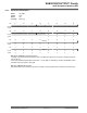


41.8.2 SPI Mode Register
Name: SPI_MR
Offset: 0x04
Reset: 0x0
Property: Read/Write
This register can only be written if the WPEN bit is cleared in theSPI W
rite Protection Mode Register .
Bit 31 30 29 28 27 26 25 24
DLYBCS[7:0]
Access
R/W R/W R/W R/W R/W R/W R/W R/W
Reset 0 0 0 0 0 0 0 0
Bit 23 22 21 20 19 18 17 16
PCS[3:0]
Access
R/W R/W R/W R/W
Reset 0 0 0 0
Bit 15 14 13 12 11 10 9 8
Access
Reset
Bit 7 6 5 4 3 2 1 0
LLB WDRBT MODFDIS PCSDEC PS MSTR
Access
R/W R/W R/W R/W R/W R/W
Reset 0 0 0 0 0 0
Bits 31:24 – DLYBCS[7:0] Delay Between Chip Selects
This field defines the delay between the inactivation and the activation of NPCS. The DL
YBCS time guarantees
nonoverlapping chip selects and solves bus contentions in case of peripherals having long data float times.
If DLYBCS is lower than 6, six peripheral clock periods are inserted by default.
Otherwise, the following equation determines the delay:
DelayBetweenChipSelects =
DLYBCS
f
peripheralclock
Bits 19:16 – PCS[3:0] Peripheral Chip Select
This field is only used if fixed peripheral select is active (PS = 0).
If SPI_MR.PCSDEC = 0:
PCS =
xxx0 NPCS[3:0] = 1110
PCS = xx01 NPCS[3:0] = 1101
PCS = x011 NPCS[3:0] = 1011
PCS = 0111 NPCS[3:0] = 0111
PCS = 1111 forbidden (no peripheral is selected)
(x = don’t care)
If SPI_MR.PCSDEC = 1:
NPCS[3:0] output signals = PCS.
Bit 7 – LLB Local Loopback Enable
LLB controls the local loopback on the data shift register for testing in Master mode only (MISO is internally
connected on MOSI).
Value Description
0
Local loopback path disabled.
1
Local loopback path enabled.
Bit 5 – WDRBT W
ait Data Read Before Transfer
SAM E70/S70/V70/V71 Family
Serial Peripheral Interface (SPI)
© 2019 Microchip T
echnology Inc.
Datasheet
DS60001527D-page 992