
Datasheet


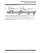


Figure 41-4. SPI Transfer Format (NCPHA = 0, 8 bits per transfer)
SPCK
(CPOL = 0)
SPCK
(CPOL = 1)
1 2 3 4 5 7
MOSI
(from master)
MISO
(from slave)
NSS
(to slave)
SPCK cycle (for reference)
8
MSB
MSB
LSB
LSB
6
6
5
5
4
4
3
3
1
1
* Not defined.
2
2
6
*
41.7.3 Master Mode Operations
When configured in Master mode, the SPI operates on the clock generated by the internal programmable baud rate
generator
. It fully controls the data transfers to and from the slave(s) connected to the SPI bus. The SPI drives the
chip select line to the slave and the serial clock signal (SPCK).
The SPI features two holding registers, the Transmit Data Register (SPI_TDR) and the Receive Data Register
(SPI_RDR), and a single shift register. The holding registers maintain the data flow at a constant rate.
After enabling the SPI, a data transfer starts when the processor writes to SPI_TDR. The written data is immediately
transferred into the internal shift register and the transfer on the SPI bus starts. While the data in the shift register is
shifted on the MOSI line, the MISO line is sampled and shifted into the shift register. Data cannot be loaded in
SPI_RDR without transmitting data. If there is no data to transmit, dummy data can be used (SPI_TDR filled with
ones). If SPI_MR.WDRBT is set, transmission can occur only if SPI_RDR has been read. If Receiving mode is not
required, for example when communicating with a slave receiver only (such as an LCD), the receive status flags in
the SPI Status register (SPI_SR) can be discarded.
Before writing SPI_TDR, SPI_MR.PCS must be set in order to select a slave.
If new data is written in SPI_TDR during the transfer, it is kept in SPI_TDR until the current transfer is completed.
Then, the received data is transferred from the shift register to SPI_RDR, the data in SPI_TDR is loaded in the shift
register and a new transfer starts.
As soon as SPI_TDR is written, the Transmit Data Register Empty (TDRE) flag in SPI_SR is cleared. When the data
written in SPI_TDR is loaded into the shift register, TDRE in SPI_SR is set. The TDRE flag is used to trigger the
Transmit DMA channel.
See the figure below.
The end of transfer is indicated by the TXEMPTY flag in SPI_SR. If a transfer delay (DLYBCT) is greater than 0 for
the last transfer, TXEMPTY is set after the completion of this delay. The peripheral clock can be switched off at this
time.
Note: When the SPI is enabled, the TDRE and TXEMPTY flags are set.
SAM E70/S70/V70/V71 Family
Serial Peripheral Interface (SPI)
© 2019 Microchip T
echnology Inc.
Datasheet
DS60001527D-page 977