
Datasheet
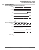


31.20.1 PMC System Clock Enable Register
Name: PMC_SCER
Offset: 0x0000
Property: Write-only
This register can only be written if the WPEN bit is cleared in the PMC W
rite Protection Mode Register.
Bit 31 30 29 28 27 26 25 24
Access
Reset
Bit 23 22 21 20 19 18 17 16
Access
Reset
Bit 15 14 13 12 11 10 9 8
PCK7 PCK6 PCK5 PCK4 PCK3 PCK2 PCK1 PCK0
Access
Reset
Bit 7 6 5 4 3 2 1 0
USBCLK
Access
Reset
Bits 8, 9, 10, 11, 12, 13, 14, 15 – PCK Programmable Clock x Output Enable
Value Description
0
No effect.
1
Enables the corresponding Programmable Clock output.
Bit 5 – USBCLK Enable USB FS Clock
Value Description
0
No effect.
1
Enables USB FS clock.
SAM E70/S70/V70/V71 Family
Power Management Controller (PMC)
© 2019 Microchip T
echnology Inc.
Datasheet
DS60001527D-page 265