
Datasheet


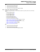


23.5.3 Supply Controller Mode Register
Name: SUPC_MR
Offset: 0x08
Reset: 0x00005A00
Property: Read/Write
Bit 31 30 29 28 27 26 25 24
KEY[7:0]
Access
R/W R/W R/W R/W R/W R/W R/W R/W
Reset 0 0 0 0 0 0 0 0
Bit 23 22 21 20 19 18 17 16
OSCBYPASS BKUPRETON
Access
R/W R/W
Reset 0 0
Bit 15 14 13 12 11 10 9 8
ONREG BODDIS BODRSTEN
Access
R/W R/W R/W
Reset 1 0 1
Bit 7 6 5 4 3 2 1 0
Access
Reset
Bits 31:24 – KEY[7:0] Password Key
Value Name Description
0xA5
PASSWD Writing any other value in this field aborts the write operation.
Bit 20 – OSCBYPASS Oscillator Bypass
Note: This bit is located in the
VDDIO domain.
Value Description
0
(NO_EFFECT): No effect. Clock selection depends on the value of SUPC_CR.XTALSEL.
1
(BYPASS): The 32.768 kHz crystal oscillator is bypassed if SUPC_CR.XTALSEL is set. OSCBYPASS
must be set prior to setting XT
ALSEL.
Bit 17 – BKUPRETON SRAM On In Backup Mode
Value Description
0
SRAM (Backup) switched off in Backup mode.
1
SRAM (Backup) switched on in Backup mode.
Note: This bit is located in the
VDDIO domain.
Bit 14 – ONREG V
oltage Regulator Enable
Note: This bit is located in the VDDIO domain.
Value Description
0
(ONREG_UNUSED): Internal voltage regulator is not used (external power supply is used).
1
(ONREG_USED): Internal voltage regulator is used.
Bit 13 – BODDIS Brownout Detector Disable
Note: This bit is located in the
VDDIO domain.
Value Description
0
(ENABLE): The core brownout detector is enabled.
SAM E70/S70/V70/V71 Family
Supply Controller (SUPC)
© 2019 Microchip T
echnology Inc.
Datasheet
DS60001527D-page 168