
Datasheet
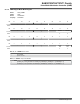


51.7.37 PWM Comparison x Value Update Register
Name: PWM_CMPVUPDx
Offset: 0x0134 + x*0x10 [x=0..7]
Reset: –
Property: Write-only
This register acts as a double buffer for the CV and CVM values. This prevents an unexpected comparison x match.
Only the first
16 bits (channel counter size) of field CVUPD are significant.
CAUTION
The write of the register PWM_CMPVUPDx must be followed by a write of the register
PWM_CMPMUPDx.
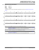
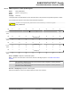
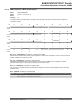
Bit 31 30 29 28 27 26 25 24
CVMUPD
Access
W
Reset –
Bit 23 22 21 20 19 18 17 16
CVUPD[23:16]
Access
W W W W W W W W
Reset 0 0 0 0 0 0 0 0
Bit 15 14 13 12 11 10 9 8
CVUPD[15:8]
Access
W W W W W W W W
Reset 0 0 0 0 0 0 0 0
Bit 7 6 5 4 3 2 1 0
CVUPD[7:0]
Access
W W W W W W W W
Reset 0 0 0 0 0 0 0 –
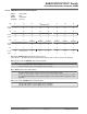
Bit 24 – CVMUPD Comparison x V
alue Mode Update
Note: This bit is not relevant if the counter of the channel 0 is left-aligned (CALG = 0 in PWM Channel Mode
Register)
Value Description
0
The comparison x between the counter of the channel 0 and the comparison x value is performed
when this counter is incrementing.
1
The comparison x between the counter of the channel 0 and the comparison x value is performed
when this counter is decrementing.
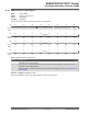
Bits 23:0 – CVUPD[23:0] Comparison x V
alue Update
Define the comparison x value to be compared with the counter of the channel 0.
SAM E70/S70/V70/V71 Family
Pulse W
idth Modulation Controller (PWM)
©
2019 Microchip Technology Inc.
Datasheet
DS60001527D-page 1636