
Datasheet
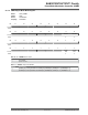

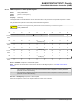


51.7.35 PWM Write Protection Status Register
Name: PWM_WPSR
Offset: 0xE8
Reset: 0x00000000
Property: Read-only
Bit 31 30 29 28 27 26 25 24
WPVSRC[15:8]
Access
R R R R R R R R
Reset 0 0 0 0 0 0 0 0
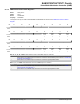
Bit 23 22 21 20 19 18 17 16
WPVSRC[7:0]
Access
R R R R R R R R
Reset 0 0 0 0 0 0 0 0
Bit 15 14 13 12 11 10 9 8
WPHWS5 WPHWS4 WPHWS3 WPHWS2 WPHWS1 WPHWS0
Access
R R R R R R
Reset 0 0 0 0 0 0
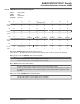
Bit 7 6 5 4 3 2 1 0
WPVS WPSWS5 WPSWS4 WPSWS3 WPSWS2 WPSWS1 WPSWS0
Access
R R R R R R R
Reset 0 0 0 0 0 0 0
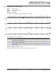
Bits 31:16 – WPVSRC[15:0] W
rite Protect Violation Source
When WPVS = 1, WPVSRC indicates the register address offset at which a write access has been attempted.
Bits 8, 9, 10, 11, 12, 13 – WPHWSx Write Protect HW Status
Value Description
0
The HW write protection x of the register group x is disabled.
1
The HW write protection x of the register group x is enabled.
Bit 7 – WPVS W
rite Protect Violation Status
Value Description
0
No write protection violation has occurred since the last read of PWM_WPSR.
1
At least one write protection violation has occurred since the last read of PWM_WPSR. If this violation
is an unauthorized attempt to write a protected register
, the associated violation is reported into field
WPVSRC.
Bits 0, 1, 2, 3, 4, 5 – WPSWSx W
rite Protect SW Status
Value Description
0
The SW write protection x of the register group x is disabled.
1
The SW write protection x of the register group x is enabled.
SAM E70/S70/V70/V71 Family
Pulse W
idth Modulation Controller (PWM)
© 2019 Microchip T
echnology Inc.
Datasheet
DS60001527D-page 1634