
Datasheet


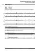

43.7.8 TWIHS Filter Register
Name: TWIHS_FILTR
Offset: 0x44
Reset: 0x00000000
Property: Read/Write
TWIHS digital input filtering follows a majority decision based on three samples from SDA/SCL lines at peripheral
clock frequency
.
Bit 31 30 29 28 27 26 25 24
Access
Reset
Bit 23 22 21 20 19 18 17 16
Access
Reset
Bit 15 14 13 12 11 10 9 8
THRES[2:0]
Access
Reset 0 0 0
Bit 7 6 5 4 3 2 1 0
PADFCFG PADFEN FILT
Access
Reset 0 0 0
Bits 10:8 – THRES[2:0] Digital Filter Threshold
Value Description
0
No filtering applied on TWIHS inputs.
1–7
Maximum pulse width of spikes to be suppressed by the input filter, defined in peripheral clock cycles.
Bit 2 – PADFCFG P
AD Filter Config
See the electrical characteristics section for filter configuration details.
Bit 1 – PADFEN PAD Filter Enable
Value Description
0
PAD analog filter is disabled.
1
PAD analog filter is enabled. (The analog filter must be enabled if High-speed mode is enabled.)
Bit 0 – FILT RX Digital Filter
Value Description
0
No filtering applied on TWIHS inputs.
1
TWIHS input filtering is active (only in Standard and Fast modes)
SAM E70/S70/V70/V71 Family
T
wo-wire Interface (TWIHS)
© 2019 Microchip T
echnology Inc.
Datasheet
DS60001527D-page 1100