
Datasheet
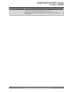


19.4.8 Peripheral Clock Configuration Register
Name: CCFG_PCCR
Offset: 0x0118
Reset: 0x00022224
Property: Read/Write
Bit 31 30 29 28 27 26 25 24
Access
Reset
Bit 23 22 21 20 19 18 17 16
I2SC1CC I2SC0CC TC0CC
Access
Reset 0 0 0
Bit 15 14 13 12 11 10 9 8
Access
Reset
Bit 7 6 5 4 3 2 1 0
Access
Reset
Bit 22 – I2SC1CC I2SC1 Clock Configuration
Value Description
0
Peripheral clock of I2SC1 is used.
1
GCLK is used.
Bit 21 – I2SC0CC I2SC0 Clock Configuration
Value Description
0
Peripheral clock of I2SC0 is used.
1
GCLK is used.
Bit 20 – TC0CC TC0 Clock Configuration
Value Description
0
PCK6 is used (default).
1
PCK7 is used.
SAM E70/S70/V70/V71 Family
Bus Matrix (MA
TRIX)
© 2019 Microchip T
echnology Inc.
Datasheet
DS60001527D-page 110