
Datasheet


SAM3X / SAM3A [DATASHEET]
Atmel-11057C-ATARM-SAM3X-SAM3A-Datasheet_23-Mar-15
438
25.12.3 Reload User Configuration Wait State
The user may change any of the configuration parameters by writing the SMC user interface.
When detecting that a new user configuration has been written in the user interface, the SMC inserts a wait state
before starting the next access. The so called “Reload User Configuration Wait State” is used by the SMC to load
the new set of parameters to apply to next accesses.
The Reload Configuration Wait State is not applied in addition to the Chip Select Wait State. If accesses before
and after re-programming the user interface are made to different devices (Chip Selects), then one single Chip
Select Wait State is applied.
On the other hand, if accesses before and after writing the user interface are made to the same device, a Reload
Configuration Wait State is inserted, even if the change does not concern the current Chip Select.
25.12.3.1 User Procedure
To insert a Reload Configuration Wait State, the SMC detects a write access to any SMC_MODE register of the
user interface. If only the timing registers are modified (SMC_SETUP, SMC_PULSE, SMC_CYCLE registers) in
the user interface, the user must validate the modification by writing the SMC_MODE register, even if no change
was made on the mode parameters.
25.12.3.2 Slow Clock Mode Transition
A Reload Configuration Wait State is also inserted when the Slow Clock Mode is entered or exited, after the end of
the current transfer (see “Slow Clock Mode” on page 448).
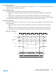
25.12.4 Read to Write Wait State
Due to an internal mechanism, a wait cycle is always inserted between consecutive read and write SMC accesses.
This wait cycle is referred to as a read to write wait state in this document.
This wait cycle is applied in addition to chip select and reload user configuration wait states when they are to be
inserted. See Figure 25-13 on page 435.
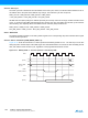
25.13 Data Float Wait States
Some memory devices are slow to release the external bus. For such devices, it is necessary to add wait states
(data float wait states) after a read access:
before starting a read access to a different external memory,
before starting a write access to the same device or to a different external one.
The Data Float Output Time (t
DF
) for each external memory device is programmed in the TDF_CYCLES field of the
SMC_MODE register for the corresponding chip select. The value of TDF_CYCLES indicates the number of data
float wait cycles (between 0 and 15) before the external device releases the bus, and represents the time allowed
for the data output to go to high impedance after the memory is disabled.
Data float wait states do not delay internal memory accesses. Hence, a single access to an external memory with
long t
DF
will not slow down the execution of a program from internal memory.
The data float wait states management depends on the READ_MODE and the TDF_MODE fields of the
SMC_MODE register for the corresponding chip select.
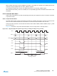
25.13.1 READ_MODE
Setting READ_MODE to 1 indicates to the SMC that the NRD signal is responsible for turning off the tri-state
buffers of the external memory device. The Data Float Period then begins after the rising edge of the NRD signal
and lasts TDF_CYCLES MCK cycles.
When the read operation is controlled by the NCS signal (READ_MODE = 0), the TDF field gives the number of
MCK cycles during which the data bus remains busy after the rising edge of NCS.