
Datasheet


435
SAM3X / SAM3A [DATASHEET]
Atmel-11057C-ATARM-SAM3X-SAM3A-Datasheet_23-Mar-15
When multiple chip selects (external SRAM) are handled, it is possible to configure the scrambling function per
chip select using the OCMS field in the SMC_TIMINGS registers.
To scramble the NAND Flash contents, the SRSE field must be set in the SMC_OCMS register.
When NAND Flash memory content is scrambled, the on-chip SRAM page buffer associated for the transfer is also
scrambled.
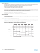
25.12 Automatic Wait States
Under certain circumstances, the SMC automatically inserts idle cycles between accesses to avoid bus contention
or operation conflict.
25.12.1 Chip Select Wait States
The SMC always inserts an idle cycle between 2 transfers on separate chip selects. This idle cycle ensures that
there is no bus contention between the de-activation of one device and the activation of the next one.
During chip select wait state, all control lines are turned inactive: NBS0 to NBS1, NWR0 to NWR1, NCS[0..7], NRD
lines are all set to 1.
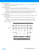
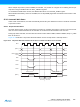
Figure 25-13 illustrates a chip select wait state between access on Chip Select 0 and Chip Select 2.
Figure 25-13. Chip Select Wait State between a Read Access on NCS0 and a Write Access on NCS2
A[23:2]
NBS0, NBS1,
A0,A1
NCS0
NRD_CYCLE
Chip Select
Wait State
NWE_CYCLE
MCK
NCS2
NRD
NWE
D[15:0]
Read to Write
Wait State