
Datasheet


SAM3X / SAM3A [DATASHEET]
Atmel-11057C-ATARM-SAM3X-SAM3A-Datasheet_23-Mar-15
434
25.10.6 Reset Values of Timing Parameters
Table 25-7 gives the default value of timing parameters at reset.
25.10.7 Usage Restriction
The SMC does not check the validity of the user-programmed parameters. If the sum of SETUP and PULSE
parameters is larger than the corresponding CYCLE parameter, this leads to unpredictable behavior of the SMC.
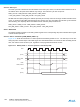
25.10.7.1 For Read Operations
Null but positive setup and hold of address and NRD and/or NCS can not be guaranteed at the memory interface
because of the propagation delay of theses signals through external logic and pads. If positive setup and hold
values must be verified, then it is strictly recommended to program non-null values so as to cover possible skews
between address, NCS and NRD signals.
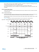
25.10.7.2 For Write Operations
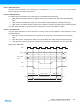
If a null hold value is programmed on NWE, the SMC can guarantee a positive hold of address, byte select lines,
and NCS signal after the rising edge of NWE. This is true for WRITE_MODE = 1 only. See “Early Read Wait State”
on page 436.
For read and write operations: a null value for pulse parameters is forbidden and may lead to unpredictable
behavior.
In read and write cycles, the setup and hold time parameters are defined in reference to the address bus. For
external devices that require setup and hold time between NCS and NRD signals (read), or between NCS and
NWE signals (write), these setup and hold times must be converted into setup and hold times in reference to the
address bus.
25.11 Scrambling/Unscrambling Function
The external data bus D[15:0] can be scrambled in order to prevent intellectual property data located in off-chip
memories from being easily recovered by analyzing data at the package pin level of either microcontroller or
memory device.
The scrambling and unscrambling are performed on-the-fly without additional wait states.
The scrambling method depends on two user-configurable key registers, SMC_KEY1 and SMC_KEY2. These key
registers are only accessible in write mode.
The key must be securely stored in a reliable non-volatile memory in order to recover data from the off-chip
memory. Any data scrambled with a given key cannot be recovered if the key is lost.
The scrambling/unscrambling function can be enabled or disabled by programming the SMC_OCMS register.
One bit is dedicated to enable/disable NAND Flash scrambling and one bit is dedicated enable/disable scrambling
the off chip SRAM. When at least one external SRAM is scrambled, the SMSC field must be set in the
SMC_OCMS register.
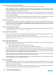
Table 25-7. Reset Values of Timing Parameters
Register Reset Value Description
SMC_SETUP 0x01010101 All setup timings are set to 1
SMC_PULSE 0x01010101 All pulse timings are set to 1
SMC_CYCLE 0x00030003
The read and write operation last 3 Master Clock cycles
and provide one hold cycle
WRITE_MODE 1 Write is controlled with NWE
READ_MODE 1 Read is controlled with NRD