
Datasheet


SAM3X / SAM3A [DATASHEET]
Atmel-11057C-ATARM-SAM3X-SAM3A-Datasheet_23-Mar-15
432
25.10.3.3 Write Cycle
The write cycle time is defined as the total duration of the write cycle, that is, from the time where address is set on
the address bus to the point where address may change. The total write cycle time is equal to:
NWE_CYCLE = NWE_SETUP + NWE_PULSE + NWE_HOLD
= NCS_WR_SETUP + NCS_WR_PULSE + NCS_WR_HOLD
All NWE and NCS (write) timings are defined separately for each chip select as an integer number of Master Clock
cycles. To ensure that the NWE and NCS timings are coherent, the user must define the total write cycle instead of
the hold timing. This implicitly defines the NWE hold time and NCS (write) hold times as:
NWE_HOLD = NWE_CYCLE - NWE_SETUP - NWE_PULSE
NCS_WR_HOLD = NWE_CYCLE - NCS_WR_SETUP - NCS_WR_PULSE
25.10.4 Write Mode
The WRITE_MODE parameter in the SMC_MODE register of the corresponding chip select indicates which signal
controls the write operation.
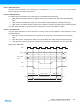
25.10.4.1 Write is Controlled by NWE (WRITE_MODE = 1)
Figure 25-11 shows the waveforms of a write operation with WRITE_MODE set to 1. The data is put on the bus
during the pulse and hold steps of the NWE signal. The internal data buffers are turned out after the NWE_SETUP
time, and until the end of the write cycle, regardless of the programmed waveform on NCS.
Figure 25-11. WRITE_MODE = 1. The write operation is controlled by NWE
MCK
D[15:0]
NCS
A
[23:2]
NBS0, NBS1,
A0, A1
NWE,
NWR0, NWR1