
Datasheet


431
SAM3X / SAM3A [DATASHEET]
Atmel-11057C-ATARM-SAM3X-SAM3A-Datasheet_23-Mar-15
25.10.3 Write Waveforms
The write protocol is similar to the read protocol. It is depicted in Figure 25-10. The write cycle starts with the
address setting on the memory address bus.
25.10.3.1 NWE Waveforms
The NWE signal is characterized by a setup timing, a pulse width and a hold timing.
1. NWE_SETUP: the NWE setup time is defined as the setup of address and data before the NWE falling
edge.
2. NWE_PULSE: The NWE pulse length is the time between NWE falling edge and NWE rising edge.
3. NWE_HOLD: The NWE hold time is defined as the hold time of address and data after the NWE rising edge.
The NWE waveforms apply to all byte-write lines in Byte Write access mode: NWR0 to NWR3.
25.10.3.2 NCS Waveforms
The NCS signal waveforms in write operation are not the same as those applied in read operations, but are
separately defined:
1. NCS_WR_SETUP: the NCS setup time is defined as the setup time of address before the NCS falling
edge.
2. NCS_WR_PULSE: the NCS pulse length is the time between NCS falling edge and NCS rising edge.
3. NCS_WR_HOLD: the NCS hold time is defined as the hold time of address after the NCS rising edge.
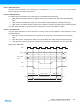
Figure 25-10. Write Cycle
A
[23:2]
NBS0, NBS1,
A0, A1
NCS
NWE_SETUP NWE_PULSE NWE_HOLD
MCK
NWE
NCS_WR_SETUP NCS_WR_PULSE NCS_WR_HOLD
NWE_CYCLE