
Datasheet


1445
SAM3X / SAM3A [DATASHEET]
Atmel-11057C-ATARM-SAM3X-SAM3A-Datasheet_23-Mar-15
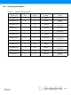
50. Revision History
In the table that follows, the most recent version of the document appears first.
Table 50-1. SAM3X/SAM3A Datasheet Rev. 11057C Revision History
Issue Date Comments
23-Mar-15
Reformatted document; editorial changes throughout; renamed package 100-ball LFBGA to 100-ball TFBGA
throughout
“Description”
Changed “9x general-purpose 32-bit timers, an RTC” to “three 3-channel general-purpose 32-bit timers, a low-power
RTC, a low-power RTT, 256-bit General Purpose Backup Registers”
Added paragraph relating to low-power modes
Section 1. “Features”
Updated description of “Low-power Modes”
Under “Peripherals”:
- changed “32-bit Real Time Timer (RTT) and RTC” to “32-bit low-power Real-time Timer (RTT) and low-power Real-
time Clock (RTC)”
- added bullet “256-bit General Purpose Backup Registers (GPBR)”
Table 1-1 ”Configuration Summary”: added footnote “Available only on SAM3X8H in LFBGA217 package (not
commercially available)” to SDRAM Controller
Section 2. “SAM3X/A Block Diagram”: in all block diagrams (Figure 2-1 through Figure 2-4),
- renumbered three Timer Counter blocks as 0-1-2 (were previously A-B-C)
- corrected JTAG/SWD pin name “TDO” to “TDO/TRACESWO”
- updated SPI signal names
Figure 2-1 ”SAM3A4/8C (100 pins) Block Diagram”: removed duplicated DMA cells from blocks SPI0, SSC, and
HSMCI
Section 3. “Signal Description”
Table 3-1 ”Signal Description List”: updated SPI signal names
Section 3.1 “Design Considerations”: updated to provide title and number of referenced application note
Section 4. “Package and Pinout”
Table 4-2 ”100-ball TFBGA SAM3X4/8E Package and Pinout”: renamed ‘WAKEUP’ to ‘FWUP’ for ball H5
Section 5. “Power Considerations”
Added Section 5.2 “Power-up Considerations”
Figure 5-2 “Single Supply”: corrected main supply range “1.8V-3.6V” to “1.62–3.6 V”
Figure 5-4 “Backup Batteries Used”: corrected main supply range “1.8V-3.6V” to “1.62–3.6 V”
Updated Section 5.7 “Wake-up Sources”
Updated Section 5.8 “Fast Startup”
Section 6. “Input/Output Lines”
Table 6-1 ”System I/O Configuration Pin List”: changed header in first column from “SYSTEM_IO Bit Number” to
“CCFG_SYSIO Bit No.”
Section 6.6 “ERASE Pin”: in first paragraph, added details relative to reprogramming Flash content; in last sentence,
changed “asserting the pin to low does not erase the Flash” to “asserting the pin to high does not erase the Flash”
Removed Section 7. “Processor and Architecture”