
Datasheet


1329
SAM3X / SAM3A [DATASHEET]
Atmel-11057C-ATARM-SAM3X-SAM3A-Datasheet_23-Mar-15
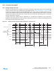
43.6.10 ADC Timings
Each ADC has its own minimal Startup Time that is programmed through the field STARTUP in the Mode Register,
ADC_MR.
A minimal Tracking Time is necessary for the ADC to guarantee the best converted final value between two
channel selections. This time has to be programmed through the TRACKTIM bit field in the Mode Register,
ADC_MR.
When the gain, offset or differential input parameters of the analog cell change between two channels, the analog
cell may need a specific settling time before starting the tracking phase. In that case, the controller automatically
waits during the settling time defined in the “ADC Mode Register”. Obviously, if the ANACH option is not set, this
time is unused.
Warning: No input buffer amplifier to isolate the source is included in the ADC. This must be taken into
consideration to program a precise value in the TRACKTIM field. See the product ADC Characteristics section.
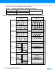
43.6.11 Buffer Structure
The PDC read channel is triggered each time a new data is stored in ADC_LCDR register. The same structure of
data is repeatedly stored in ADC_LCDR register each time a trigger event occurs. Depending on user mode of
operation (ADC_MR, ADC_CHSR, ADC_SEQR1, ADC_SEQR2) the structure differs. Each data transferred to
PDC buffer, carried on a half-word (16-bit), consists of last converted data right aligned and when TAG is set in
ADC_EMR register, the 4 most significant bits are carrying the channel number thus allowing an easier post-
processing in the PDC buffer or better checking the PDC buffer integrity.