
Datasheet


SAM9G20
DS60001516A-page 578 2017 Microchip Technology Inc.
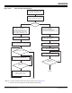
The flowchart in Figure 34-12 shows how to manage a multiple write block transfer with the PDC. Polling or interrupt method can be used
to wait for the end of write according to the contents of the MCI_IMR.
Figure 34-12: Multiple Write Functional Flow Diagram
Note 1: It is assumed that this command has been correctly sent (see Figure 34-9).
2: This field is also accessible in the MCI Block Register (MCI_BLKR).
Configure the PDC channel
MCI_TPR = Data Buffer Address to write
MCI_TCR = BlockLength/4
Send WRITE_MULTIPLE_BLOCK
command
(1)
Read status register MCI_SR
Poll the bit
BLKE = 0?
Ye s
MCI_PTCR = TXTEN
Set the PDCMODE bit
MCI_MR |= PDCMODE
Set the block length (in bytes)
MCI_BLKR |= (BlockLength << 16)
(2)
Set the block count (if necessary)
MCI_BLKR |= (BlockCount << 0)
No
Poll the bit
NOTBUSY = 0?
Ye s
RETURN
No
Send STOP_TRANSMISSION
command
(1)
Send SELECT/DESELECT_CARD
command
(1)
to select the card
Send SET_BLOCKLEN command
(1)