
Datasheet


SAM9G20
DS60001516A-page 192 2017 Microchip Technology Inc.
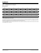
Figure 21-2: Write Burst, 32-bit SDRAM Access
21.5.2 SDRAM Controller Read Cycle
The SDRAM Controller allows burst access, incremental burst of unspecified length or single access. In all cases, the SDRAM Controller
keeps track of the active row in each bank, thus maximizing performance of the SDRAM. If row and bank addresses do not match the
previous row/bank address, then the SDRAM controller automatically generates a precharge command, activates the new row and starts
the read command. To comply with the SDRAM timing parameters, additional clock cycles on SDCK are inserted between precharge and
active commands (t
RP
) and between active and read command (t
RCD
). These two parameters are set in the configuration register of the
SDRAM Controller. After a read command, additional wait states are generated to comply with the CAS latency (1, 2 or 3 clock delays
specified in the configuration register).
For a single access or an incremented burst of unspecified length, the SDRAM Controller anticipates the next access. While the last value
of the column is returned by the SDRAM Controller on the bus, the SDRAM Controller anticipates the read to the next column and thus
anticipates the CAS latency. This reduces the effect of the CAS latency on the internal bus.
For burst access of specified length (4, 8, 16 words), access is not anticipated. This case leads to the best performance. If the burst is
broken (border, busy mode, etc.), the next access is handled as an incrementing burst of unspecified length.
SDCK
SDCS
RAS
CAS
SDRAMC_A[12:0]
D[31:0]
t
RCD
= 3
Dna
SDWE
Dnb Dnc Dnd
Dne
Dnf
Dng Dnh
Dni Dnj
Dnk Dnl
Row n col a col b col c col d col e col f col g col h col i col j col k col l