
Datasheet


1033
SAM9263 [DATASHEET]
Atmel-6249N-ATARM-SAM9263-Datasheet_14-Mar-16
46.8 USB Transceiver Characteristics
46.9 EBI Timings
46.9.1 SMC Timing Conditions
Timings are given assuming a capacitance load on data, control and address pads as defined in Table 46-17.
In the tables that follow, MCK period is represented by t
CPMCK
.
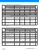
Table 46-16. USB Electrical Characteristics
Symbol Parameter Conditions Min Typ Max Unit
Input Levels
V
IL
Low Level 0.8 V
V
IH
High Level 2.0 V
V
DI
Differential Input Sensitivity |(D+) - (D-)| 0.2 V
V
CM
Differential Input Common Mode
Range
0.8 2.5 V
C
IN
Transceiver capacitance Capacitance to ground on each line 9.18 pF
I
lkg
Hi-Z State Data Line Leakage 0V < V
IN
< 3.3V - 10 + 10 µA
R
EXT
Recommended External USB Series
Resistor
In series with each USB pin with ±5% 27 Ω
Output Levels
V
OL
Low Level Output Measured with R
L
of 1.425 kΩ tied to 3.6V 0.0 0.3 V
V
OH
High Level Output Measured with R
L
of 14.25 kΩ tied to GND 2.8 3.6 V
V
CRS
Output Signal Crossover Voltage
Measurement conditions described in
Figure 46-16
1.3 2.0 V
Pull-up and Pull-down Resistor
R
PUI
Bus Pull-up Resistor on Upstream Port
(idle bus)
0.900 1.575 kΩ
R
PUA
Bus Pull-up Resistor on Upstream Port
(upstream port receiving)
1.425 3.090 kΩ
Table 46-17. Capacitance Load
Supply Max Min
3.3V 50 pF 0 pF
1.8V 30 pF 0 pF