
Datasheet


1040
32117D–AVR-01/12
AT32UC3C
33.7.40 Channel Period Register
Name:
CPRD
Access Type: Read/Write
Offset: 0x20C + [ch_num * 0x20]
Reset Value: 0x00000000
This register can only be written if the WPSWS3 and WPHWS3 bits are cleared in ”Write Protect Status Register” on page
1030.
Only the first 20 bits (channel counter size) are significant.
• CPRD: Channel Period
If the waveform is left-aligned, then the output waveform period depends on the channel counter source clock and can be
calculated:
– By using the PWM internal clock (CCK) divided by an X given prescaler value (with X being 1, 2, 4, 8, 16, 32, 64, 128,
256, 512, or 1024). The resulting period formula will be:
– By using the PWM internal clock (CCK) divided by one of both DIVA or DIVB divider, the formula becomes,
respectively:
or
If the waveform is center-aligned, then the output waveform period depends on the channel counter source clock and can
be calculated:
– By using the PWM internal clock (CCK) divided by an X given prescaler value (with X being 1, 2, 4, 8, 16, 32, 64, 128,
256, 512, or 1024). The resulting period formula will be:
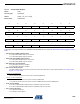
31 30 29 28 27 26 25 24
- -------
23 22 21 20 19 18 17 16
CPRD
15 14 13 12 11 10 9 8
CPRD
76543210
CPRD
XCPRD×()
CCK
-------------------------------
CRPD DIVA×()
CCK
------------------------------------------
CRPD DIVB×()
CCK
------------------------------------------
2 X CPRD××()
CCK
---------------------------------------- -