
Datasheet


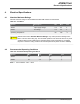

Pin
#
Name Type Description Programmable
Pull Up Resistor
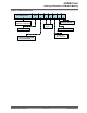
6 NC - No connect. -
7 NC - No connect. -
8 NC - No connect. -
9 GND_1 - GND. -
10 SPI_CFG I Tie to VDDIO through a 1 MΩ resistor to enable the
SPI interface.
No
11 WAKE I Host Wake control. Can be used to wake-up the
module from Doze mode. Connect to a host GPIO.
Yes
12 GND_2 - GND. -
13 IRQN O ATWINC15x0-MR210xB Device Interrupt output.
Connect to host interrupt input pin.
Yes
14 UART_TXD O UART Transmit Output from ATWINC15x0-MR210xB
Added debug.
Yes
15 SPI_RXD I SPI MOSI (Master Out, Slave In) pin. Yes
16 SPI_SSN I SPI Slave Select. Active-low. Yes
17 SPI_TXD O SPI MISO (Master In, Slave Out) pin. Yes
18 SPI_SCK I SPI Clock. Yes
19 UART_RXD I UART Receive input to ATWINC15x0-MR210xB.
Added debug.
Yes
20 VBATT - Battery power supply. -
21 GPIO_1/RTC I General Purpose I/O / RTC. Yes
22 CHIP_EN I Module enable. High level enables the module; low
level places module in Power-Down mode. Connect
to a host output that defaults low at power-up. If the
host output is tri-stated, add a 1 MΩ pull down
resistor to ensure a low level at power-up.
No
23 VDDIO - I/O Power Supply. Must match host I/O voltage. -
24 1P3V_TP - 1.3V VDD Core Test Point. Decouple with 10 µF, and
0.01 µF to GND.
-
25 GPIO_3 I/O General purpose I/O. Yes
26 GPIO_4 I/O General purpose I/O. Yes
27 GPIO_5 I/O General purpose I/O. Yes
28 GND_3 - GND. -
29 PADDLE GND - GND. -
ATWINC15x0
Pin Description
© 2018 Microchip Technology Inc.
Datasheet
DS70005304C-page 9