
Datasheet


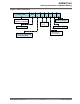


3. Pin Description
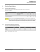
Figure 3-1. Pin Diagram
VBAT
GPIO_1
CHIP_EN
VDDIO
1
21
22
23
24
25
26
27
28
11
12
13
14
15
16
17
18
10
19
20
GPIO_3
GPIO_4
GPIO_5
GND_3
GND_1
NC
NC
NC
NC
RESET_N
I2C_SDA
I2C_SCL
GPIO_6
SPI_CFG
WAKE
GND_2
IRQN
UART_TXD
SPI_MOSI
SPI_SSN
SPI_MISO
SPI_SCK
UART_RXD
1P3V_TP
2
3
4
5
6
7
8
9
ATWINC15x0-MR210
29
PADDLE
GND
(Bottom)
Table 3-1. ATWINC15x0-MR210xB Pin Description
Pin
#
Name Type Description Programmable
Pull Up Resistor
1 GPIO_6 I/O General purpose I/O. Yes
2 I2C_SCL I/O I2C Slave Clock. Currently used only for development
debug. Leave unconnected.
Yes
3 I2C_SDA I/O I2C Slave Data. Currently used only for development
debug. Leave unconnected.
Yes
4 RESET_N I Active-Low Hard Reset. When this pin is asserted
low, the module will be placed in the reset state.
When this pin is asserted high, the module will be out
of reset and will function normally. Connect to a host
output that defaults low at power up. If the host output
is tri-stated, add a 1 MΩ pull down resistor to ensure
a low level at power-up.
No
5 NC - No connect. -
ATWINC15x0
Pin Description
© 2018 Microchip Technology Inc.
Datasheet
DS70005304C-page 8