
Datasheet


12. Design Considerations
This section provides the guidelines on placement and routing to achieve the best performance.
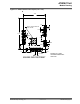
12.1 ATWINC15x0-MR210PB Placement and Routing Guidelines
• The module must be placed on the main board – the printed antenna area must overlap with the
carrier board. The portion of the module containing the antenna should not go outside the edge of
the main board. The antenna is designed to work properly when it is sitting directly on top of a
1.5mm thick printed circuit board.
• If the module is placed at the edge of the main board, a minimum 22mm by 5mm area directly
under the antenna must be clear of all metal on all layers of the board. “In-land” placement is
acceptable; however deepness of keep-out area must grove to: module edge to main board edge
plus 5mm. DO NOT PLACE THE MODULE IN THE MIDDLE OF THE MAIN BOARD OR FAR
AWAY FROM THE MAIN BOARD EDGE.
• Keep away from the antenna, as far as possible, large metal objects to avoid electromagnetic field
blocking
• Do not enclose the antenna within a metal shield
• Keep any components which may radiate noise or signals within the 2.4GHz-2.5GHz frequency
band as far away from the antenna as possible, or better yet, shield those components. Any noise
radiated from the main board in this frequency band will degrade the sensitivity of the module.
Figure 12-1. ATWINC15x0-MR210PB Placement Reference
Best Case
Worst Case
System Ground Plane
(a)
(b)
Keep out area.
Microchip
Microchip
12.2 Printed PCB Antenna Performance of ATWINC15x0-MR210PB
The printed PCB antenna on the ATWINC15x0-MR210PB is a meandered Inverted F Antenna (IFA). The
antenna is fed via matching network, which is matched for the module installed on a 1.5mm thick main
ATWINC15x0
Design Considerations
© 2018 Microchip Technology Inc.
Datasheet
DS70005304C-page 32