
Datasheet


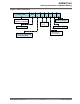


Table of Contents
1. Ordering Information and Module Marking................................................................ 5
2. Block Diagram........................................................................................................... 7
3. Pin Description.......................................................................................................... 8
4. Electrical Specifications...........................................................................................10
4.1. Absolute Maximum Ratings........................................................................................................10
4.2. Recommended Operating Conditions........................................................................................ 10
5. CPU and Memory Subsystems................................................................................11
5.1. Processor................................................................................................................................... 11
5.2. Memory Subsystem....................................................................................................................11
5.3. Non-volatile Memory (eFuse)..................................................................................................... 11
6. WLAN Subsystem................................................................................................... 13
6.1. MAC........................................................................................................................................... 13
6.2. PHY............................................................................................................................................14
6.3. Radio..........................................................................................................................................14
7. External Interfaces...................................................................................................18
7.1. Interfacing with the Host Microcontroller.................................................................................... 18
7.2. SPI Interface...............................................................................................................................19
7.3. UART Interface...........................................................................................................................21
8. Power Consumption................................................................................................ 23
8.1. Description of Device States...................................................................................................... 23
8.2. Current Consumption in Various Device States......................................................................... 23
8.3. Restrictions for Power States..................................................................................................... 24
8.4. Power-up/down Sequence......................................................................................................... 24
8.5. Digital I/O Pin Behavior During Power-up Sequences............................................................... 25
8.6. Module Reset............................................................................................................................. 26
9. Notes On Interfacing to the ATWINC15x0-MR210xB.............................................. 27
9.1. Programmable Pull Up Resistors............................................................................................... 27
10. Schematic Design Information.................................................................................28
10.1. Application Schematic................................................................................................................ 28
11. Module Drawing.......................................................................................................29
11.1. Module Footprint........................................................................................................................ 30
12. Design Considerations............................................................................................ 32
12.1. ATWINC15x0-MR210PB Placement and Routing Guidelines....................................................32
12.2. Printed PCB Antenna Performance of ATWINC15x0-MR210PB............................................... 32
© 2018 Microchip Technology Inc.
Datasheet
DS70005304C-page 3