
Datasheet

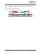


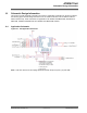


Table 8-2. Power-up/down Sequence Timing
Parameter Min. Max. Units Description Notes
t
A
0 ms VBATT rise to VDDIO
rise
VBATT and VDDIO can rise
simultaneously or can be tied
together. VDDIO must not rise
before VBATT.
t
B
0 ms VDDIO rise to CHIP_EN
rise
CHIP_EN must not rise before
VDDIO. CHIP_EN must be driven
high or low, not left floating.
t
C
5 ms CHIP_EN rise to
RESETN rise
This delay is needed because the
XO clock must stabilize before
RESETN removal. RESETN must
be driven high or low, not left
floating.
t
A’
0 ms VDDIO fall to VBATT fall VBATT and VDDIO can fall
simultaneously or can be tied
together. VBATT must not fall
before VDDIO.
t
B’
0 ms CHIP_EN fall to VDDIO
fall
VDDIO must not fall before
CHIP_EN. CHIP_EN and RESETN
can fall simultaneously.
t
C’
0 ms RESETN fall to VDDIO
fall
VDDIO must not fall before
RESETN. RESETN and CHIP_EN
can fall simultaneously.
8.5 Digital I/O Pin Behavior During Power-up Sequences
The following table represents digital I/O Pin states corresponding to device power modes.
Table 8-3. Digital I/O Pin Behavior in Different Device States
Device state VDDIO CHIP_EN RESETN Output
driver
Input
driver
Pull up/down
resistor (96kΩ)
Power-Down:
core supply off
High Low Low Disabled (Hi-Z) Disabled Disabled
Power-on Reset:
core supply on, hard reset
on
High High Low Disabled (Hi-Z) Disabled Enabled
Power-On Default:
core supply on, the device
is out of reset but not
programmed yet
High High High Disabled (Hi-Z) Enabled Enabled
ATWINC15x0
Power Consumption
© 2018 Microchip Technology Inc.
Datasheet
DS70005304C-page 25