
Datasheet

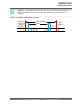


Device State Code Rate
Output
power, dBm
Current Consumption
1
IVBATT IVDDIO
ON_Doze N/A N/A 380µA <10µA
Power_Down N/A N/A <0.5µA <3.5µA
Note:
1. Measured conditions: VBATT @ 3.3V, VDDIO@ 3.3V, temp. 25°C.
8.3 Restrictions for Power States
When no power is supplied to the device, for example, the DC/DC Converter output and VDDIO are both
off (at ground potential), a voltage cannot be applied to the device pins because each pin contains an
ESD diode from the pin to supply. This diode will turn on when a voltage higher than one diode drop is
supplied to the pin.
If a voltage must be applied to the signal pads while the chip is in a low-power state, the VDDIO supply
must be on, so the SLEEP or Power_Down state must be used.
Similarly, to prevent the pin-to-ground diode from turning on, do not apply a voltage that is more than one
diode drop below ground to any pin.
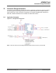
8.4 Power-up/down Sequence
The power-up/down sequence for ATWINC15x0-MR210xB is shown in the Following Figure. The timing
parameters are provided in following the table.
Figure 8-1. Power Up/Down Sequence
VBATT
VDDIO
CHIP_EN
RESETN
t
A
t
B
t
C
XO Clock
t
B'
t
A'
t
C'
ATWINC15x0
Power Consumption
© 2018 Microchip Technology Inc.
Datasheet
DS70005304C-page 24