
Datasheet

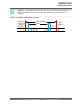


Parameter Symbol Min. Max. Units
Clock Low Pulse Width t
WL
4 —
ns
Clock High Pulse Width t
WH
5 —
Clock Rise Time t
LH
0 7
Clock Fall Time t
HL
0 7
TXD Output Delay
3
t
ODLY
4 9 from SCK fall
12.5 from SCK
rise
RXD Input Setup Time t
ISU
1 —
RXD Input Hold Time t
IHD
5 —
SSN Input Setup Time t
SUSSN
3 —
SSN Input Hold Time t
HDSSN
5.5 —
Note:
1. Timing is applicable to all SPI modes
2. Maximum clock frequency specified is limited by the SPI Slave interface internal design, actual
maximum clock frequency can be lower and depends on the specific PCB layout
3. Timing based on 15pF output loading
7.3 UART Interface
The ATWINC15x0-MR210xB supports the Universal Asynchronous Receiver/Transmitter (UART)
interface. This interface should be used for debug purposes only. The UART is available on pins 14 and
19. The UART is compatible with the RS-232 standard, and the ATWINC15x0-MR210xB operates as
Data Terminal Equipment (DTE). It has a two-pin RXD/TXD interface.
The default configuration for accessing the UART interface of ATWINC15x0-MR210xB is mentioned
below:
• Baud rate: 115200
• Data: 8 bit
• Parity: None
• Stop bit: 1 bit
• Flow control: None
It also has RX and TX FIFOs, which ensure reliable high-speed reception and low software overhead
transmission. FIFO size is 4 x 8 for both RX and TX direction. The UART also has status registers
showing the number of received characters available in the FIFO and various error conditions, as well the
ability to generate interrupts based on these status bits.
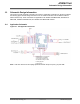
An example of the UART receiving or transmitting a single packet is shown in the following figure. This
example shows 7-bit data (0x45), odd parity, and two stop bits.
ATWINC15x0
External Interfaces
© 2018 Microchip Technology Inc.
Datasheet
DS70005304C-page 21