
Datasheet


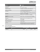


The red lines in the following figure correspond to Clock Phase = 0 and the blue lines correspond to Clock
Phase = 1.
Figure 7-2. SPI Slave Clock Polarity and Clock Phase Timing
z
z z
z
SCK
CPOL = 0
CPOL = 1
SSN
RXD/TXD
(MOSI/MISO)
CPHA = 0
CPHA = 1
2 3 4 5 6 7 8
1 2 3 4 5 6 7
1
8
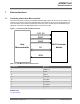
The SPI timing is provided in the following figure and table.
Figure 7-3. SPI Timing Diagram (SPI Mode CPOL=0, CPHA=0)
t
LH
SCK
TXD
RXD
t
WH
t
HL
t
WL
t
ODLY
t
ISU
t
IHD
f
SCK
SSN
t
SUSSN
t
HDSSN
Table 7-4. SPI Slave Timing Parameters
1
Parameter Symbol Min. Max. Units
Clock Input Frequency
2
f
SCK
— 48 MHz
ATWINC15x0
External Interfaces
© 2018 Microchip Technology Inc.
Datasheet
DS70005304C-page 20