
Datasheet


7.2 SPI Interface
7.2.1 Overview
The ATWINC15x0-MR210xB has a Serial Peripheral Interface (SPI) that operates as an SPI slave. The
SPI interface can be used for control and for serial I/O of 802.11 data. The SPI pins are mapped as
shown in the following table. The SPI is a full-duplex slave-synchronous serial interface that is available
immediately following reset when pin 10 (SPI_CFG) is tied to VDDIO.
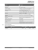
Table 7-2. SPI Interface Pin Mapping
Pin # SPI function
10 CFG: Must be tied to VDDIO
16 SSN: Active-Low Slave Select
15 MOSI(RXD): Serial Data Receive
18 SCK: Serial Clock
17 MISO(TXD): Serial Data Transmit
When the SPI is not selected, that is, when SSN is high, the SPI interface will not interfere with data
transfers between the serial-master and other serial-slave devices. When the serial slave is not selected,
its transmitted data output is buffered, resulting in a high impedance drive onto the MISO line.
The SPI interface responds to a protocol that allows an external host to read or write any register in the
chip as well as initiate DMA transfers.
The SPI SSN, MOSI, MISO, and SCK pins of the ATWINC15x0-MR210xB have internal programmable
pull-up resistors. These resistors should be programmed to be disabled; otherwise, if any of the SPI pins
are driven to a low level while the ATWINC15x0-MR210xB is in the low power sleep state, the current will
flow from the VDDIO supply through the pull-up resistors, increasing the current consumption of the
module.
Related Links
9.1 Programmable Pull Up Resistors
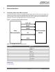
7.2.2 SPI Timing
The SPI Slave interface supports four standard modes as determined by the Clock Polarity (CPOL) and
Clock Phase (CPHA) settings. These modes are illustrated in the following table and figure.
Table 7-3. SPI Slave Modes
Mode CPOL CPHA
0 0 0
1 0 1
2 1 0
3 1 1
Note: The ATWINC15x0 firmware uses “SPI MODE 0” to communicate with the host.
ATWINC15x0
External Interfaces
© 2018 Microchip Technology Inc.
Datasheet
DS70005304C-page 19