
Datasheet


5. CPU and Memory Subsystems
5.1 Processor
The ATWINC15x0-MR210xB modules have a Cortus APS3 32-bit processor. This processor performs
many of the MAC functions, including but not limited to the association, authentication, power
management, security key management, and MSDU aggregation/de-aggregation. In addition, the
processor provides flexibility for various modes of operation, such as STA and AP modes.
5.2 Memory Subsystem
The APS3 core uses a 128KB instruction/boot ROM along with a 160KB instruction RAM and a 64KB
data RAM. The ATWINC15x0-MR210xB modules come populated with either 4Mb or 8Mb of Flash
memory depending on the module model that is ordered. This memory can be used for system software.
See Table 1-1 for more information. In addition, the device uses a 128KB shared RAM, accessible by the
processor and MAC, which allows the APS3 core to perform various data management tasks on the TX
and RX data packets.
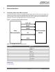
5.3 Non-volatile Memory (eFuse)
The ATWINC15x0-MR210xB modules have 768 bits of non-volatile eFuse memory that can be read by
the CPU after device reset. This non-volatile one-time-programmable (OTP) memory can be used to store
customer-specific parameters, such as MAC address; various calibration information, such as TX power,
crystal frequency offset, etc.; and other software-specific configuration parameters. The eFuse is
partitioned into six 128-bit banks. Each bank has the same bitmap (see following figure). The purpose of
the first 80 bits in each bank is fixed, and the remaining 48 bits are general-purpose software dependent
bits, or reserved for future use. Since each bank can be programmed independently, this allows for
several updates of the device parameters following the initial programming; for example, if the MAC
address has to be changed, Bank 1 has to be programmed with the new MAC address along with the
values of TX gain correction and frequency offset if they are used and programmed in Bank 0. The
contents of Bank 0 have to be invalidated in this case by programming the invalid bit in the Bank 0. This
will allow the firmware to use the MAC address. By default, all the ATWINC15x0-MR210xB modules are
programmed with the MAC address and the frequency offset bits of Bank 0.
ATWINC15x0
CPU and Memory Subsystems
© 2018 Microchip Technology Inc.
Datasheet
DS70005304C-page 11