ATWINC15x0 ATWINC15x0-MR210xB IEEE® 802.11 b/g/n SmartConnect IoT Module Introduction The ATWINC15x0-MR210xB is a low power consumption 802.11 b/g/n IoT (Internet of Things) module,specifically optimized for low power IoT applications. The module integrates Power Amplifier (PA), Low-Noise Amplifier (LNA), Switch, Power Management, and a printed antenna or a micro co-ax (u.FL) connector for an external antenna resulting in a small form factor (21.7 x 14.7 x 2.1 mm) design.
ATWINC15x0 • • • • • • • • • • • Operating temperature range from -40°C to +85°C. RF performance at room temperature of 25oC with a 2-3 db change at boundary conditions I/O operating voltage of 2.7V to 3.6V Built-in 26 MHz crystal Integrated Flash memory for system software Power Save modes – 4 µA Power-Down mode typical at 3.
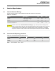
Table of Contents 1. Ordering Information and Module Marking................................................................ 5 2. Block Diagram........................................................................................................... 7 3. Pin Description.......................................................................................................... 8 4. Electrical Specifications...........................................................................................10 4.1. 4.2.
ATWINC15x0 12.3. ATWINC15x0-MR210UB Placement and Routing Guidelines................................................... 35 12.4. Module Assembly Considerations.............................................................................................. 36 13. Reflow Profile Information....................................................................................... 37 13.1. 13.2. 13.3. 13.4. Storage Condition...........................................................................................
ATWINC15x0 Ordering Information and Module Marking 1. Ordering Information and Module Marking Following table describes the ordering details for the ATWINC15x0-MR210xB modules. Table 1-1. Ordering Details Model Number Ordering Code1 Package Dimension No. Description of Pins Regulatory Certification ATWINC1500MR210PB ATWINC1500MR210PBXXXX 21.7 x 14.7 x 2.
ATWINC15x0 Ordering Information and Module Marking Figure 1-1. Marking Information ATWINC15x0 - MR ATWINC1500: 4Mb Flash ATWINC1510: 8Mb Flash 2 1 0 Software Version Reserved 1 0 MR Industrial Module Revision Letter P: PCB Antenna U: uFL Connector 1: No OTA / with shield 2: OTA with shield © 2018 Microchip Technology Inc.
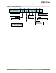
ATWINC15x0 Block Diagram 2. Block Diagram Figure 2-1. ATWINC15x0-MR210xB Module Block Diagram Printed 2.4 GHz Antenna or u.FL 2.4 GHz External Antenna Connector VBAT VDDIO SPI_CFG SPI RX/TX BAL UN Wi-Fi ® ATWINC15x0 SoC GPIO 3 GPIO 4 GPIO 5 GPIO 6 IRQN Chip_EN WAKE 26 MHz crystal RESET GN D © 2018 Microchip Technology Inc.
ATWINC15x0 Pin Description Pin Description Figure 3-1. Pin Diagram ATWINC15x0-MR210 9 8 GND_2 IRQN 12 UART_TXD 14 15 7 NC NC 6 NC 5 NC 4 RESET_N 3 2 1 I2C_SCL I2C_SDA GPIO_6 GND_3 27 GND_1 28 23 VDDIO 1P3V_TP GPIO_5 22 CHIP_EN UART_RXD 18 19 21 SPI_SCK 16 17 GPIO_1 SPI_SSN SPI_MISO 13 20 SPI_MOSI 29 PADDLE GND (Bottom) GPIO_3 GPIO_4 WAKE 10 11 24 25 26 SPI_CFG VBAT 3. Table 3-1.
ATWINC15x0 Pin Description Pin # Name Type Description Programmable Pull Up Resistor 6 NC - No connect. - 7 NC - No connect. - 8 NC - No connect. - 9 GND_1 - GND. - 10 SPI_CFG I Tie to VDDIO through a 1 MΩ resistor to enable the SPI interface. No 11 WAKE I Host Wake control. Can be used to wake-up the module from Doze mode. Connect to a host GPIO. Yes 12 GND_2 - GND. 13 IRQN O ATWINC15x0-MR210xB Device Interrupt output. Connect to host interrupt input pin.
ATWINC15x0 Electrical Specifications 4. Electrical Specifications 4.1 Absolute Maximum Ratings Absolute maximum ratings for the ATWINC15x0-MR210xB modules are listed below. Table 4-1. Conditions Symbol Description Min. Max. Unit VBATT Input supply voltage -0.3 5.0 V VDDIO I/O voltage -0.3 4.2 V -40 +85 oC Operating Temperature CAUTION 4.2 Stresses listed under "Absolute Maximum Ratings" may cause permanent damage to the device. This is a stress rating only.
ATWINC15x0 CPU and Memory Subsystems 5. CPU and Memory Subsystems 5.1 Processor The ATWINC15x0-MR210xB modules have a Cortus APS3 32-bit processor. This processor performs many of the MAC functions, including but not limited to the association, authentication, power management, security key management, and MSDU aggregation/de-aggregation. In addition, the processor provides flexibility for various modes of operation, such as STA and AP modes. 5.
ATWINC15x0 CPU and Memory Subsystems Figure 5-1. eFuse Bitmap Flags 8 Bank 0 F 48 MAC ADDR TX Gain Correc tion 8 G 1 15 Freq. Offset 7 Used 1 Used 1 MAC ADDR Used 4 Reserved 3 Version 1 Invalid Used 1 16 FO Bank 1 Bank 2 Bank 3 Bank 4 Bank 5 128 Bits © 2018 Microchip Technology Inc.
ATWINC15x0 WLAN Subsystem 6. WLAN Subsystem The WLAN subsystem is composed of the Media Access Controller (MAC) and the Physical Layer (PHY). The following two subsections describe the MAC and PHY in detail. 6.1 MAC 6.1.1 Description The ATWINC15x0-MR210xB MAC is designed to operate at low power while providing high data throughput. The IEEE 802.11 MAC functions are implemented with a combination of dedicated datapath engines, hardwired control logic, and a low-power, high-efficiency microprocessor.
ATWINC15x0 WLAN Subsystem • • • • Support for IEEE802.11i and WFA security with key management: – WEP 64/128 – WPA-TKIP – 128-bit WPA2 CCMP (AES) Advanced power management: – Standard 802.11 Power Save Mode RTS-CTS and CTS-self support Supports either STA or AP mode in the infrastructure basic service set mode 6.2 PHY 6.2.1 Description The ATWINC1500B WLAN PHY is designed to achieve reliable and power-efficient physical layer communication specified by IEEE 802.
ATWINC15x0 WLAN Subsystem Feature Description Host Interface SPI Dimension 21.7 x 14.7 x 2.1 mm Frequency Range 2.412GHz ~ 2.472GHz (2.4GHz ISM Band) Number of Channels 11 for North America, and 13 for Europe Modulation 802.11b: DQPSK, DBPSK, CCK 802.11g/n: OFDM /64-QAM,16-QAM, QPSK, BPSK Data Rate 802.11b: 1, 2, 5.5, 11Mbps 802.11g: 6, 9, 12, 18, 24, 36, 48, 54Mbps 6.3.1 Data Rate (20MHz, normal GI, 800ns) 802.11n: 6.5, 13, 19.5, 26, 39, 52, 58.
ATWINC15x0 WLAN Subsystem Parameter Sensitivity 802.11b Sensitivity 802.11g Sensitivity 802.11n (BW=20MHz) Maximum Receive Signal Level Adjacent Channel Rejection Description Minimum Typical 1Mbps DSS -95 2Mbps DSS -90 5.5Mbps DSS -92 11Mbps DSS -86 6Mbps OFDM -90 9Mbps OFDM -89 12Mbps OFDM -88 18Mbps OFDM -85 24Mbps OFDM -83 36Mbps OFDM -80 48Mbps OFDM -76 54Mbps OFDM -74 MCS 0 -89 MCS 1 -87 MCS 2 -85 MCS 3 -82 MCS 4 -77 MCS 5 -74 MCS 6 -72 MCS 7 -70.
ATWINC15x0 WLAN Subsystem Parameter Cellular Blocker Immunity 6.3.2 Description Minimum Typical 776-794MHz CDMA -14 824-849MHz GSM -10 880-915MHz GSM -10 1710-1785MHz GSM -15 1850-1910MHz GSM -15 1850-1910MHz WCDMA -24 1920-1980MHz WCDMA -24 Maximum Unit dBm Transmitter Performance Table 6-3. Transmitter Performance Parameter Description Minimum Typical Maximum Unit Frequency — 2,412 — 2,472 MHz 802.11b 1Mbps — 17.5 — 802.11b 11Mbps — 18.5 — 802.11g 6Mbps — 17.
ATWINC15x0 External Interfaces 7. External Interfaces 7.1 Interfacing with the Host Microcontroller This section describes interfacing the ATWINC15x0-MR210xB module with the host microcontroller. The interface is comprised of a slave SPI and additional control signals, as shown in the following figure. For more information on SPI interface specification and timing, refer to the SPI Interface. Additional control signals are connected to the GPIO/IRQ interface of the microcontroller. Figure 7-1.
ATWINC15x0 External Interfaces 7.2 SPI Interface 7.2.1 Overview The ATWINC15x0-MR210xB has a Serial Peripheral Interface (SPI) that operates as an SPI slave. The SPI interface can be used for control and for serial I/O of 802.11 data. The SPI pins are mapped as shown in the following table. The SPI is a full-duplex slave-synchronous serial interface that is available immediately following reset when pin 10 (SPI_CFG) is tied to VDDIO. Table 7-2.
ATWINC15x0 External Interfaces The red lines in the following figure correspond to Clock Phase = 0 and the blue lines correspond to Clock Phase = 1. Figure 7-2. SPI Slave Clock Polarity and Clock Phase Timing CPOL = 0 SCK CPOL = 1 SSN RXD/TXD (MOSI/MISO) z CPHA = 0 1 2 z CPHA = 1 1 3 2 4 5 3 4 6 5 7 6 8 7 z 8 z The SPI timing is provided in the following figure and table. Figure 7-3.
ATWINC15x0 External Interfaces Parameter Symbol Min. Max. Units Clock Low Pulse Width tWL 4 — Clock High Pulse Width tWH 5 — Clock Rise Time tLH 0 7 Clock Fall Time tHL 0 7 TXD Output Delay3 tODLY 4 9 from SCK fall 12.5 from SCK rise RXD Input Setup Time tISU 1 — RXD Input Hold Time tIHD 5 — SSN Input Setup Time tSUSSN 3 — SSN Input Hold Time tHDSSN 5.5 — ns Note: 1. Timing is applicable to all SPI modes 2.
ATWINC15x0 External Interfaces Important: UART2 supports RTS and CTS flow control. The UART RTS and UART CTS MUST be connected to the host MCU UART and enabled for the UART interface to be functional. Figure 7-4. Example of UART RX of TX Packet Previous Packets or Leading Idle Bits © 2018 Microchip Technology Inc.
ATWINC15x0 Power Consumption 8. Power Consumption 8.1 Description of Device States The ATWINC15x0-MR210xB has several device states: • • • • • ON_Transmit – Device is actively transmitting an 802.11 signal. Highest output power and nominal current consumption. ON_Receive – Device is actively receiving an 802.11 signal. Lowest sensitivity and nominal current consumption.
ATWINC15x0 Power Consumption Device State Code Rate Output power, dBm Current Consumption 1 ON_Doze N/A N/A 380µA <10µA Power_Down N/A N/A <0.5µA <3.5µA IVBATT IVDDIO Note: 1. 8.3 Measured conditions: VBATT @ 3.3V, VDDIO@ 3.3V, temp. 25°C.
ATWINC15x0 Power Consumption Table 8-2. Power-up/down Sequence Timing Parameter Min. Max. Units Description Notes 0 ms VBATT rise to VDDIO rise VBATT and VDDIO can rise simultaneously or can be tied together. VDDIO must not rise before VBATT. 0 ms VDDIO rise to CHIP_EN rise CHIP_EN must not rise before VDDIO. CHIP_EN must be driven high or low, not left floating. 5 ms CHIP_EN rise to RESETN rise This delay is needed because the XO clock must stabilize before RESETN removal.
ATWINC15x0 Power Consumption 8.6 Device state VDDIO CHIP_EN RESETN Output driver Input driver Pull up/down resistor (96kΩ) On Sleep/ On Transmit/ On Receive: core supply on, device programmed by firmware High High Programmed by firmware for each pin: Enabled or Disabled Opposite of Output Driver state Programmed by firmware for each pin: Enabled or Disabled High Module Reset If a module reset is performed, the RESETN pin must be pulsed low for a minimum of 1µ second.
ATWINC15x0 Notes On Interfacing to the ATWINC15x0-MR210xB 9. Notes On Interfacing to the ATWINC15x0-MR210xB 9.1 Programmable Pull Up Resistors The ATWINC15x0-MR210xB provides programmable pull up resistors on various pins. The purpose of these resistors is to keep any unused input pins from floating, which can cause excess current to flow through the input buffer from the VDDIO supply. Any unused module pin on the ATWINC15x0-MR210xB should leave these pull up resistors enabled so the pin will not float.
ATWINC15x0 Schematic Design Information 10. Schematic Design Information This section provides schematic information for reference. Application schematics for SPI are provided in the following figure. Module design information such as module schematics can be obtained under an NDA from Microchip. These schematics are applicable to the ATWINC1500-MR210PB, ATWINC1510MR210PB, ATWINC1500-MR210UB, and ATWINC1510-MR210UB modules. 10.1 Application Schematic Figure 10-1.
ATWINC15x0 Module Drawing 11. Module Drawing This section provides information about the module package outline drawings. Figure 11-1. Module Drawing - ATWINC15x0-MR210PB (unit = mm) Metal Shield NOTE: THIS PAD MUST BE SOLDERED TO GND. PCB Metal Shield MODULE SIDE VIEW MODULE TOP VIEW © 2018 Microchip Technology Inc.
ATWINC15x0 Module Drawing Figure 11-2. Module Drawings – ATWINC15x0-MR210UB (unit = mm) Metal Shield NOTE: THIS PAD MUST BE SOLDERED TO GND. PCB Metal Shield MODULE BOTTOM VIEW MODULE SIDE VIEW MODULE TOP VIEW 11.1 NOT TO SCALE Rev. 2 Module Footprint This section provides the outline drawing for the recommended footprint for the ATWINC15x0-MR210xB module.
ATWINC15x0 Module Drawing Figure 11-3. Module Solder Pad Footprint (unit = mm). 14.73 1.9 NOTE: THIS PAD MUST BE TIED TO GND. 0.8 1.016 Pitch 2.032 21.72 1.016 Pitch 4.064 3.70 1.016 Pitch 3.70 6.00 4.42 3.68 2.67 1.9 2.67 3.048 1.016 Pitch SOLDER PAD FOOTPRINT © 2018 Microchip Technology Inc. Datasheet Drawing not to scale. Untoleranced dimensions. Units=mm.
ATWINC15x0 Design Considerations 12. Design Considerations This section provides the guidelines on placement and routing to achieve the best performance. 12.1 ATWINC15x0-MR210PB Placement and Routing Guidelines • • • • • The module must be placed on the main board – the printed antenna area must overlap with the carrier board. The portion of the module containing the antenna should not go outside the edge of the main board.
ATWINC15x0 Design Considerations board. Main board thickness deviation by ±1mm changes RX/TX performance by ±1dB maximum, referring to RX/TX performance with a default antenna matching network and installed on 1.5mm thick main board. Measured peak antenna gain is -0.3dBi. Antenna Radiation Pattern Following figures illustrate the Antenna Radiation Patterns. Figure 12-2. Antenna Radiation Pattern when Phi = 0 degree © 2018 Microchip Technology Inc.
ATWINC15x0 Design Considerations Figure 12-3. Antenna Radiation Pattern when Phi = 90 degree © 2018 Microchip Technology Inc.
ATWINC15x0 Design Considerations Figure 12-4. Antenna Radiation Pattern when Theta = 90 degree 12.3 ATWINC15x0-MR210UB Placement and Routing Guidelines The ATWINC15x0-MR210UB module has an Ultra Small Miniature RF Connector (u.FL) for the external antenna. The choice of antenna is limited to the antenna types for which the module was tested and approved. For a list of tested and approved antennas that may be used with the module, refer to the respective country in 14. Regulatory Approval.
ATWINC15x0 Design Considerations 12.3.1 Recommended External Antenna for ATWINC15x0-MR210UB Whip Antenna (Part number: RN-SMA-4) along with a 10cm length RF cable assembly (u.FL to SMA) has been used for the certification of ATWINC15x0-MR210UB. It is recommended to use the same or similar external antenna in design. 12.4 Module Assembly Considerations The ATWINC15x0-MR210xB modules are assembled with an EMI Shield to ensure compliance with EMI emission and immunity rules.
ATWINC15x0 Reflow Profile Information 13. Reflow Profile Information This chapter provides guidelines for reflow processes in getting the Microchip module soldered to the customer’s design. For more information on reflow process guidelines, refer to Solder Reflow Recommendation Application Note (DS00233D). 13.1 Storage Condition 13.1.1 Moisture Barrier Bag Before Opening A moisture barrier bag must be stored in a temperature of less than 30°C with humidity under 85% RH.
ATWINC15x0 Reflow Profile Information temperature. The targeted solder joint temperature for the Sn-Ag-Cu solder should be ~235°C. For larger or sophisticated boards with a large mix of components, it is also important to ensure that the temperature difference across the board is less than 10 degrees to minimize board warpage. The maximum temperature at the component body should not exceed the MSL3 qualification specification. 13.4.
ATWINC15x0 Reflow Profile Information recommended to pay attention to heat-proof the proximity of the mounted parts and junctions and use the best nozzle for rework that is suited to the module size. © 2018 Microchip Technology Inc.
ATWINC15x0 Regulatory Approval 14. Regulatory Approval Regulatory Approvals received.
ATWINC15x0 Regulatory Approval 14.1 United States The ATWINC1500-MR210PB, ATWINC1510-MR210PB, ATWINC1500-MR210UB, and ATWINC1510MR210UB modules have received Federal Communications Commission (FCC) CFR47 Telecommunications, Part 15 Subpart C “Intentional Radiators” single-modular approval in accordance with Part 15.212 Modular Transmitter approval.
ATWINC15x0 Regulatory Approval Contains Transmitter Module FCC ID: 2ADHKATWINC1510 or Contains FCC ID: 2ADHKATWINC1510 This device complies with Part 15 of the FCC Rules. Operation is subject to the following two conditions: (1) this device may not cause harmful interference, and (2) this device must accept any interference received, including interference that may cause undesired operation.
ATWINC15x0 Regulatory Approval 14.1.2 RF Exposure All transmitters regulated by FCC must comply with RF exposure requirements. KDB 447498 General RF Exposure Guidance provides guidance in determining whether proposed or existing transmitting facilities, operations or devices comply with limits for human exposure to Radio Frequency (RF) fields adopted by the Federal Communications Commission (FCC). From the FCC Grant: Output power listed is conducted.
ATWINC15x0 Regulatory Approval For the ATWINC1500-MR210UB module: Contains IC: 20266-WINC1500UB For the ATWINC1510-MR210UB module: Contains IC: 20266-WINC1500UB User Manual Notice for License-Exempt Radio Apparatus (from Section 8.
ATWINC15x0 Regulatory Approval This radio transmitter (identify the device by certification number, or model number if Category II) has been approved by Industry Canada to operate with the antenna types listed below with the maximum permissible gain and required antenna impedance for each antenna type indicated. Antenna types not included in this list, having a gain greater than the maximum gain indicated for that type, are strictly prohibited for use with this device.
ATWINC15x0 Regulatory Approval Table 14-1. European Compliance Testing (ATWINC15x0-MR210PB) Certification Standards Safety EN60950-1:2006/A11:2009/ A1:2010/ A12:2011/A2:2013 Health EN300328 V1.9.1/ EN62311:2008 Article Laboratory [3.1(a)] [3.1(b)] TUV Rheinland, Taiwan EN301489-17 V3.1.1 EN301489-17 V3.2.0 Radio 2017-02-20 50068130 002 EN301489-17 V2.2.1 EMC Date 10059657 001 EN301489-1 V1.9.2 EN301489-1 V2.1.1 EN301489-1 V2.2.0 Report Number EN300328 V1.9.
ATWINC15x0 Regulatory Approval 14.3.2.1 Simplified EU Declaration of Conformity Hereby, Microchip Technology Inc. declares that the radio equipment type ATWINC15x0-MR210xB is in compliance with Directive 2014/53/EU. The full text of the EU declaration of conformity for this product is available at http://www.microchip.com/ design-centers/wireless-connectivity/. 14.3.
ATWINC15x0 Regulatory Approval 005-101762 14.4.2 Helpful Web Sites Ministry of Internal Affairs and Communications (MIC): http://www.tele.soumu.go.jp/e/index.htm Association of Radio Industries and Businesses (ARIB): http://www.arib.or.jp/english/ 14.5 Korea The ATWINC15x0-MR210PB module has received certification of conformity in accordance with the Radio Waves Act.
ATWINC15x0 Regulatory Approval CCAN18LP0321T2 For the ATWINC1510-MR210PB module, due to the limited module size, the NCC mark and ID are displayed in the data sheet only and cannot be displayed on the module label: CCAN18LP0320T0 The user's manual should contain following warning (for RF device) in traditional Chinese: 注意 ! 依據 低功率電波輻射性電機管理辦法 第十二條 經型式認證合格之低功率射頻電機,非經許 可, 公司、商號或使用者均不得擅自變更頻率、加大功率或 變更原設計 之特性及功能。 第十四條 低功率射頻電機之使用不得影響飛航安全及 干擾合法通信; 經發現有干擾現象時,應立即停用,並改善至無干擾時 方得繼續使用。 前項合法通信,指依電信規定作業之無線電信。 低功率射頻電機須忍受合
ATWINC15x0 Regulatory Approval When Host system is using an approved Full Modular Approval (FMA) radio: The host must bear a label containing the statement “This device contains SRRC approved Radio module CMIIT ID: 2018DJ1305”.
ATWINC15x0 Reference Documentation and Support 15. 15.1 Reference Documentation and Support Reference Documents The following table provides the set of collateral documents to ease integration and device ramp. Table 15-1. Reference Documents Title Content ATWINC1500 MU Device Datasheet Datasheet for the ATWINC1500 SmartConnect Wi-Fi component. For more details, contact a Microchip sales representative. Platform Getting Started Guide Details on how to evaluate the WINC15X0 Network Controller Module.
ATWINC15x0 Document Revision History 16. Document Revision History Note: The datasheet revision is independent of the die revision (Revision bit in the Device Identification register of the Device Service Unit, DSU.DID.REVISION) and the device variant (last letter of the ordering number). Rev C - 09/2018 Section Changes Features Added Enterprise security feature and related note. Ordering Information and Module Marking Updated Table 1-1. Pin Description Updated Table 3-1.
ATWINC15x0 Document Revision History Section Product Description Changes • • • • • Added description information indicating that the document content is relevant to all WINC1500 Module models unless noted. Changed SSL references to TLS. Removed WAPI security. Removed UART as host interface. Editorial updates. Product Features • • • • • • Removed WAPI security. Removed UART and I2C as host interfaces. Removed Bluetooth coexistance interface. Replaced SSL with TLS. Added 26 MHz crystal.
ATWINC15x0 Document Revision History Section Changes External Interfaces • • • • Revised SPI timing information in table 7-3. Removed Bluetooth Coexistance section. Removed SDIO. Editorial updates. Power Consumption • Added Module Reset section for reset duration. Editorial updates. • 12.1 ATWINC15x0-MR210PB Placement and Routing Guidelines • • Added text for antenna types used in test and an associated table. Revised Co-Ax connector type.
ATWINC15x0 Document Revision History WLAN Subsystem Radio • Revised Transmit Performance Table 6-3. Power Consumption • Revised current table references in Table 8-1. Schematic Design Information • Updated Schematics Section 11 text and figures Figure 11-1 and Figure 11-2. Reflow Profile Information • Revised section 12 Reflow Profile Information. Reference Documents • Updated Document Reference table to include the ATWINC1500-MU datasheet.
ATWINC15x0 The Microchip Web Site Microchip provides online support via our web site at http://www.microchip.com/. This web site is used as a means to make files and information easily available to customers.
ATWINC15x0 • Neither Microchip nor any other semiconductor manufacturer can guarantee the security of their code. Code protection does not mean that we are guaranteeing the product as “unbreakable.” Code protection is constantly evolving. We at Microchip are committed to continuously improving the code protection features of our products. Attempts to break Microchip’s code protection feature may be a violation of the Digital Millennium Copyright Act.
ATWINC15x0 © 2018, Microchip Technology Incorporated, Printed in the U.S.A., All Rights Reserved. ISBN: 978-1-5224-3491-7 Quality Management System Certified by DNV ISO/TS 16949 Microchip received ISO/TS-16949:2009 certification for its worldwide headquarters, design and wafer fabrication facilities in Chandler and Tempe, Arizona; Gresham, Oregon and design centers in California ® ® and India.
Worldwide Sales and Service AMERICAS ASIA/PACIFIC ASIA/PACIFIC EUROPE Corporate Office 2355 West Chandler Blvd. Chandler, AZ 85224-6199 Tel: 480-792-7200 Fax: 480-792-7277 Technical Support: http://www.microchip.com/ support Web Address: www.microchip.