
User`s guide


MPLAB
®
IDE User’s Guide
DS51519B-page 10 © 2006 Microchip Technology Inc.
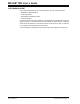
1.1.3 Components of a Microcontroller
The PICmicro MCU has program memory for the firmware, or coded instructions, to run
a program. It also has “file register” memory for storage of variables that the program
will need for computation or temporary storage. It also has a number of peripheral
device circuits on the same chip. Some peripheral devices are called I/O ports. I/O
ports are pins on the microcontroller that can be driven high or low to send signals, blink
lights, drive speakers – just about anything that can be sent through a wire. Often these
pins are bidirectional and can also be configured as inputs allowing the program to
respond to an external switch, sensor or to communicate with some external device.
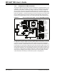
FIGURE 1-1:
PICmicro
®
MCU DATA SHEET – BLOCK DIAGRAM (EXCERPT)
In order to design such a system, it must be decided which peripherals are needed for
an application. Analog-to-Digital Converters (ADCs) allow microcontrollers to connect
to sensors and receive changing voltage levels. Serial communication peripherals
allow you to stream communications over a few wires to another microcontroller, to a
local network or to the internet. Peripherals on the PICmicro MCU called “timers” accu-
rately measure signal events and generate and capture communications signals, pro-
duce precise waveforms, even automatically reset the microcontroller if it gets “hung”
or lost due to a power glitch or hardware malfunction. Other peripherals detect if the
external power is dipping below dangerous levels so the microcontroller can store
critical information and safely shut down before power is completely lost.
PORTA
PORTB
PORTC
RA4/T0CKI
RA5/AN4/LVDIN
RB0/INT0
RC0/T1OSO/T13CKI
RC1/T1OSI/CCP2
RC2/CCP1
RC3/SCK/SCL
RC4/SDI/SDA
RC5/SDO
RC6/TX1/CK1
RC7/RX1/DT1
RA3/AN3/V
REF
+
RA2/AN2/V
REF
-
RA1/AN1
RA0/AN0
RB1/INT1
Data Latch
Data RAM
Address Latch
Address<12>
12
Bank0, F
BSR
FSR0
FSR1
FSR2
Inc/Dec
Logic
Decode
4
12 4
PCH PCL
PCLATH
8
31 Level Stack
Program Counter
Address Latch
Program
Data Latch
21
21
16
Table Pointer<21>
21
8
Data Bus<8>
Table Latch
8
IR
12
ROM Latch
RB2/INT2
RB3/INT3
PCLATU
PCU
RA6
RB4/KBI0
RB5/KBI1/PGM
RB6/KBI2/PGC
RB7/KBI3/PGD
Memory
Inc/Dec Logic