
User`s guide

PICDEM™ Z 2.4 GHz RF Card
© 2008 Microchip Technology Inc. DS51524C-page 35
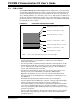
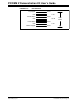
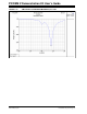
FIGURE C-13: IMPEDANCE OF THE PCB ANTENNA WITH VOLTAGE STANDING WAVE RATIO
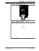
The most critical part of maintaining proper impedance is adhering to the specified
dimensions of the printed circuit board antenna (see Figure C-14). The antenna dimen-
sions, if altered, will change the specified impedance. As an example, a 1 mm variance
will shift the impedance by 5-10 MHz.
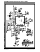
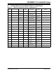
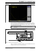
FIGURE C-14: PRINTED CIRCUIT BOARD ANTENNA DIMENSIONS
(1)
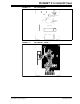
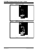
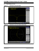
Figure C-15 and Figure C-16 illustrate simulation results of this PCB antenna. Note the
simulation results are very close to the measurements.
Note: This part has been simulated using a HFSS™ simulator by Ansoft
Corporation.
1.0
1.0
1.0
1.0
1.0
0.72
3.37
0.85
0.5
3.82
4.2
6.6
4.3
1.2
1.3
2
.
0
3.8
5.3
8.6
22.0
1.2
6.0
1.54
0.5
9.6
2.0
6.6
Note 1: Dimensions are in mm and tolerance is +/– 0.05 mm.