
User`s guide

PICDEM Z Demonstration Kit User’s Guide
DS51524C-page 28 © 2008 Microchip Technology Inc.
C.4 PCB LAYOUT
The PICDEM Z MRF24J40 2.4 GHz Daughter Card is fabricated as a four layer PCB.
The material is FR4 with signal traces in 0.5 oz copper. Figure C-4 through Figure C-9
show the individual layers from top to bottom. Figure C-10 shows the layer stack up.
The following guidelines are intended to aid users in high-frequency PCB layout
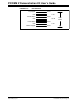
design. The printed circuit board is comprised of four basic FR4 layers: signal layout,
RF ground, power line routing and ground (see Figure C-3). The guidelines will explain
the requirements of these layers.
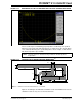
FIGURE C-3: FOUR BASIC COPPER FR4 LAYERS
• It is important to keep the original PCB thickness since any change will affect
antenna performance (see total thickness of dielectric) or microstrip lines
characteristic impedance.
• The first layer width of a 50Ω characteristic impedance microstrip line is 12 mils.
• Avoid having microstrip lines longer than 2.5 cm, since that line might get very
close to a quarter wave length of the working frequency of the board which is
3.0 cm, and start behaving as an antenna.
• Except for the antenna layout, avoid sharp corners since they can act as an
antenna. Round corners will eliminate possible future EMI problems.
• Digital lines by definition are prone to be very noisy when handling periodic
waveforms and fast clock/switching rates. Avoid laying out a RF signal close to
any digital lines.
• A via filled ground patch underneath the IC transceiver is mandatory.
• A power supply must be distributed to each pin in a star topology and low-ESR
capacitors must be placed at each pin for proper decoupling noise.
• Thorough decoupling on each power pin is beneficial for reducing in-band trans-
ceiver noise, particularly when this noise degrades performance. Usually, low
value caps (27-47 pF) combined with large value caps (100 nF) will cover a large
spectrum of frequency.
• Passive components (inductors) must be in the high-frequency category and the
SRF (Self-Resonant Frequency) should be at least two times higher than the
operating frequency.
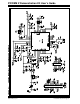
Dielectric ε = 4.5, Thickness = 7 mils
Signal Layout, Thickness = 1.8 mils
RF Ground, Thickness = 1.2 mils
Dielectric ε = 4.5, Thickness = 19 mils
Power Line Routing, Thickness = 1.2 mils
Dielectric ε = 4.5, Thickness = 7 mils
Ground, Thickness = 1.8 mils
Note: Care should be taken with all ground lines to prevent breakage.