
User`s guide

© 2008 Microchip Technology Inc. DS51524C-page 25
PICDEM
™
Z
DEMONSTRATION KIT
USER’S GUIDE
Appendix C. PICDEM™ Z 2.4 GHz RF Card
C.1 INTRODUCTION
This appendix describes the PICDEM Z MRF24J40 2.4 GHz Daughter Card. Topics
discussed in this chapter are:
• The PICDEM™ Z MRF24J40 2.4 GHz Daughter Card
•Schematic
•PCB Layout
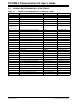
• PICDEM Z MRF24J40 Daughter Card Bill of Materials
• PCB Antenna Details
C.2 THE PICDEM™ Z MRF24J40 2.4 GHz DAUGHTER CARD
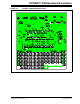
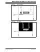
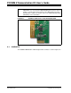
The PICDEM Z MRF24J40 2.4 GHz Daughter Card (AC163027-4) is shown in
Figure C-1. It features the MRF24J40 transceiver IC, all passive circuitry, PCB
antenna, and optional SMA connector footprint. It is designed to plug into the PICDEM
Z Motherboard, or to any application, using a 12-pin connector or Explorer 16
Development Board using the side edge connector.
The PICDEM Z MRF24J40 2.4 GHz Daughter Card is a good platform to evaluate an
inverted F-type PCB antenna. The optional SMA connector can be populated to
evaluate external antenna options or to connect to test equipment for measurement.
The PICDEM Z MRF24J40 2.4 GHz Daughter Card may be used as a reference
design. The Gerber files are available for download on the at Microchip website
http://www.microchip.com/wireless/ and on the PICDEM Z CD-ROM.
More information about the MRF24J40 IC, refer to:
“MRF24J40 2.4 GHz IEEE 802.15.4 RF Transceiver Data Sheet” (DS39776)
Features of the PICDEM Z MRF24J40 2.4 GHz Daughter Card include:
1. MRF24J40 Transceiver IC (U1): An IEEE 802.15.4 compliant transceiver IC in a
40-pin QFN package.
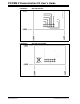
2. Daughter Card Connector (J2): Connector J2 is a 12-pin connector used to con-
nect to the PICDEM Z Motherboard or any application with a mating connector.
It supplies 3.3V power, 4-wire SPI, reset, wake and interrupt connections to the
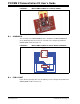
MRF24J40. The pinout is shown in Figure C-2. The 12-pin connector is a Samtec
P/N LST-106-07-F-D.
3. PCB Edge Connector (J3): Connector J3 is a 30-pin connector used to connect
to the Explorer 16 Development Board. It supplies 3.3V power, 4-wire SPI, reset,
wake and interrupt connections to the MRF24J40. The pinout is shown in
Figure C-2.
4. PCB Antenna: An inverted F-type PCB antenna.
5. Optional SMA Connector (P5): The SMA footprint may be populated with an
SMA connector for connecting to an external antenna or test equipment. The
PCB antenna is connected by default. To enable the SMA connector and disable
the PCB antenna, removed capacitor C38 and move it to position C8.