PICDEM™ Z Demonstration Kit User’s Guide © 2008 Microchip Technology Inc.
Note the following details of the code protection feature on Microchip devices: • Microchip products meet the specification contained in their particular Microchip Data Sheet. • Microchip believes that its family of products is one of the most secure families of its kind on the market today, when used in the intended manner and under normal conditions. • There are dishonest and possibly illegal methods used to breach the code protection feature.
PICDEM™ Z DEMONSTRATION KIT USER’S GUIDE Table of Contents Preface ........................................................................................................................... 1 Chapter 1. Overview 1.1 Introduction ..................................................................................................... 5 1.2 PICDEM™ Z Demonstration Kit Contents ...................................................... 5 1.3 PICDEM Z Demonstration Kit .................................................
PICDEM Z Demonstration Kit User’s Guide NOTES: DS51524C-page iv © 2008 Microchip Technology Inc.
PICDEM™ Z DEMONSTRATION KIT USER’S GUIDE Preface NOTICE TO CUSTOMERS All documentation becomes dated, and this manual is no exception. Microchip tools and documentation are constantly evolving to meet customer needs, so some actual dialogs and/or tool descriptions may differ from those in this document. Please refer to our web site (www.microchip.com) to obtain the latest documentation available. Documents are identified with a “DS” number.
PICDEM Z Demonstration Kit User’s Guide CONVENTIONS USED IN THIS GUIDE Where applicable, this manual uses the following documentation conventions: DOCUMENTATION CONVENTIONS Description Arial font: Italic characters Represents Referenced books Emphasized text A window A dialog A menu selection A field name in a window or dialog A menu path MPLAB® IDE User’s Guide ...is the only compiler...
Preface WARRANTY REGISTRATION Please complete the enclosed Warranty Registration Card and mail it promptly. Sending in the Warranty Registration Card entitles users to receive new product updates. Interim software releases are available at the Microchip web site. RECOMMENDED READING This user's guide describes how to use the PICDEM™ Z Demonstration Kit. Other useful documents are listed below. The following Microchip documents are available and recommended as supplemental reference resources.
PICDEM Z Demonstration Kit User’s Guide DEVELOPMENT SYSTEMS CUSTOMER CHANGE NOTIFICATION SERVICE Microchip’s customer notification service helps keep customers current on Microchip products. Subscribers will receive e-mail notification whenever there are changes, updates, revisions or errata related to a specified product family or development tool of interest. To register, access the Microchip web site at www.microchip.com, click on Customer Change Notification and follow the registration instructions.
PICDEM™ Z DEMONSTRATION KIT USER’S GUIDE Chapter 1. Overview 1.1 INTRODUCTION This chapter introduces the PICDEM™ Z Demonstration Kit features. This chapter discusses: • • • • • 1.2 PICDEM™ Z Demonstration Kit Contents PICDEM Z Demonstration Kit PICDEM™ Z Motherboard Wireless Daughter Boards PICDEM™ Z CD-ROM PICDEM™ Z DEMONSTRATION KIT CONTENTS The PICDEM Z Demonstration Kit (Part Number DM163027-5) contains the following items: 1. 2. 3. 4. 5. 6. Two PICDEM™ Z Motherboards Two MRF24J40MA PICDEM Z 2.
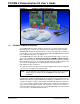
PICDEM Z Demonstration Kit User’s Guide FIGURE 1-1: 1.3 PICDEM™ Z DEMONSTRATION KIT PICDEM Z DEMONSTRATION KIT The PICDEM Z Demonstration Kit allows developers to evaluate and develop with Microchip wireless solutions. The kit provides two motherboards and two 2.4 GHz MRF24J40MA daughter boards which can be used to form a simple two node wireless network. More nodes can be added by purchasing additional PICDEM Z Demonstration Kits or individual components (see Table 1-1).
Overview 1.4 PICDEM™ Z MOTHERBOARD The PICDEM Z Motherboard contains many features to enable the evaluation and development of wireless solutions. Figure 1-2 shows the motherboard with a MRF24J40MA Module Daughter Board plugged in. Below is a description of the call outs in the figure. The motherboard schematic, PCB layout and bill of materials are available in Appendix A. 1.
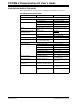
PICDEM Z Demonstration Kit User’s Guide TABLE 1-2: JUMPERS Jumper Purpose J3 To connect or disconnect the RS-232 level shifter U5 from the microcontroller USART. The pins are connected by PCB traces. JP2 To enable or disable LED D1. The pins are connected by PCB traces. JP3 To enable or disable LED D2. The pins are connected by PCB traces. JP4 To measure current draw by all circuitry past the voltage regulator U2.
Overview FIGURE 1-3: CONNECTOR J2 PINOUT J2 Microcontroller Signal Pin Pin Signal Microcontroller RB3 12 11 RB1 10 9 SCK RC3 RB2 RC4 MISO 8 7 MOSI RC5 RC0 CS 6 5 INT RB0 RC1 WAKE 4 3 RESET RC2 GND 2 1 +3.3V (Top view on Motherboard) 1.5 WIRELESS DAUGHTER BOARDS The PICDEM Z Motherboard is designed to interface with a variety of wireless daughter boards via connector J2. Connector J2 is a 12-pin connector that supplies 3.
PICDEM Z Demonstration Kit User’s Guide NOTES: DS51524C-page 10 © 2008 Microchip Technology Inc.
PICDEM™ Z DEMONSTRATION KIT USER’S GUIDE Chapter 2. Getting Started with the PICDEM™ Z Demonstration Kit 2.1 INTRODUCTION The PICDEM Z Demonstration Kit can be used with a variety of Microchip software protocol stacks or it can be used to develop proprietary protocol stacks. Microchip software protocol stacks are available as a free download, including source code, from the Microchip website: http://www.microchip.com/wireless/.
PICDEM Z Demonstration Kit User’s Guide 2.3 MICROCHIP MiWi™ PROTOCOL The MiWi Wireless Networking Protocol is a simple protocol designed for low data rate, short distance, low-cost networks. It is an application layer on top of the IEEE 802.15.4 MAC and PHY layers. The MiWi protocol provides an easy-to-use alternative for wireless communication. In particular, it targets smaller applications that have relatively small network sizes with few hops between nodes.
PICDEM™ Z DEMONSTRATION KIT USER’S GUIDE Appendix A. PICDEM™ Z Motherboard Schematics A.1 PICDEM Z MOTHERBOARD SCHEMATICS The PICDEM Z motherboard schematics are shown here. The RF daughter card schematics are found in the appendices that follow. Topic included in this appendix are: • PICDEM Z Motherboard Schematics • PICDEM Z Motherboard Bill of Materials © 2008 Microchip Technology Inc.
PICDEM Z Demonstration Kit User’s Guide 8 10 12 16 7 1 EN INVALID FORCEON FORCEOFF 14 GND V- 13 9 2 C1+ 4 C15 C2+ 6 C2- DS51524C-page 14 11 PICDEM™ Z MOTHERBOARD VCC 15 V+ 3 FIGURE A-1: © 2008 Microchip Technology Inc.
PICDEM™ Z Motherboard Schematics FIGURE A-2: PICDEM™ Z MOTHERBOARD TOP ASSEMBLY M © 2008 Microchip Technology Inc.
PICDEM Z Demonstration Kit User’s Guide FIGURE A-3: DS51524C-page 16 PICDEM™ Z MOTHERBOARD LAYER 1 © 2008 Microchip Technology Inc.
PICDEM™ Z Motherboard Schematics FIGURE A-4: PICDEM™ Z MOTHERBOARD LAYER 2 © 2008 Microchip Technology Inc.
PICDEM Z Demonstration Kit User’s Guide A.2 PICDEM Z MOTHERBOARD BILL OF MATERIALS TABLE A-1: PICDEM™ Z MOTHERBOARD BILL OF MATERIALS (BOM) Reference Description Vendor Vendor P/N D3 Diode Schottky 20V 1A SMD MELF Diodes Inc.
PICDEM™ Z DEMONSTRATION KIT USER’S GUIDE Appendix B. MRF24J40MA PICDEM Z 2.4 GHz RF Board B.1 INTRODUCTION This appendix describes the MRF24J40MA Z 2.4 GHz RF Board. Topics covered in this appendix include: • • • • B.2 MRF24J40MA PICDEM Z 2.4 GHz RF Board Schematic PCB Layout Bill of Materials MRF24J40MA PICDEM Z 2.4 GHz RF BOARD The MRF24J40MA PICDEM Z 2.4GHz RF Board (AC163028) is shown in Figure B-1. It features the MRF24J40MA transceiver module.
PICDEM Z Demonstration Kit User’s Guide FIGURE B-1: B.3 MRF24J40MA PICDEM™ Z 2.4 GHz RF BOARD SCHEMATIC The schematic for the MRF24J40MA module is available in the MRF24J40MA Data Sheet (DS70329). Figure B-2 shows the schematic of the daughter board with the MRF24J40MA module mounted on it. FIGURE B-2: MRF24J40MA PICDEM™ Z GHZ RF BOARD SCHEMATIC U1 MRF24J40MA GND RESET WAKE INT SDI SCK GND GND Vin CLKOUT CS SDO 12 11 10 9 NC 8 7 NC 1 2 3 4 5 6 11 9 7 5 3 1 P1 C1 0.1æF NC NC 12 10 8 6 4 2 B.
MRF24J40MA PICDEM Z 2.4 GHz RF Board FIGURE B-3: TOP SILKSCREEN FIGURE B-4: TOP COPPER © 2008 Microchip Technology Inc.
PICDEM Z Demonstration Kit User’s Guide DS51524C-page 22 FIGURE B-5: BOTTOM COPPER FIGURE B-6: BOTTOM SILKSCREEN © 2008 Microchip Technology Inc.
MRF24J40MA PICDEM Z 2.4 GHz RF Board B.5 BILL OF MATERIALS TABLE B-1: BILL OF MATERIALS Reference Designator Value Description U1 MRF24J40MA IEEE 802.15.4™ Transceiver Module C1 0.1 uF, 16V, X7R, 10%, 0603 Capacitor, Ceramic P1 LST-106-07-F-D Samtec Connector 2x6 Header with Locking Socket © 2008 Microchip Technology Inc.
PICDEM Z Demonstration Kit User’s Guide NOTES: DS51524C-page 24 © 2008 Microchip Technology Inc.
PICDEM™ Z DEMONSTRATION KIT USER’S GUIDE Appendix C. PICDEM™ Z 2.4 GHz RF Card C.1 INTRODUCTION This appendix describes the PICDEM Z MRF24J40 2.4 GHz Daughter Card. Topics discussed in this chapter are: • • • • • C.2 The PICDEM™ Z MRF24J40 2.4 GHz Daughter Card Schematic PCB Layout PICDEM Z MRF24J40 Daughter Card Bill of Materials PCB Antenna Details THE PICDEM™ Z MRF24J40 2.4 GHz DAUGHTER CARD The PICDEM Z MRF24J40 2.4 GHz Daughter Card (AC163027-4) is shown in Figure C-1.
PICDEM Z Demonstration Kit User’s Guide Note: The MRF24J40 SDO pin 17 defaults to a low state when nCS is high (the MRF24J40 is not selected). If the MRF24J40 Daughter Card is to share an SPI bus, a tri-state buffer can be placed on the SDO signal to provide a high-impedance signal to the SPI bus. Refer to the “MRF24J40 Data Sheet” (DS39776) for more information. FIGURE C-1: C.3 PICDEM™ Z MRF24J40 2.4 GHZ DAUGHTER CARD SCHEMATIC The PICDEM Z MRF24J40 2.
FIGURE C-2: PICDEM Z MRF24J40 2.4 GHZ DAUGHTER CARD SCHEMATIC PICDEM Z Demonstration Kit User’s Guide DS51524C-page 27 © 2008 Microchip Technology Inc.
PICDEM Z Demonstration Kit User’s Guide C.4 PCB LAYOUT The PICDEM Z MRF24J40 2.4 GHz Daughter Card is fabricated as a four layer PCB. The material is FR4 with signal traces in 0.5 oz copper. Figure C-4 through Figure C-9 show the individual layers from top to bottom. Figure C-10 shows the layer stack up. The following guidelines are intended to aid users in high-frequency PCB layout design.
PICDEM™ Z 2.4 GHz RF Card FIGURE C-4: TOP SILKSCREEN FIGURE C-5: TOP COPPER – LAYER 1 © 2008 Microchip Technology Inc.
PICDEM Z Demonstration Kit User’s Guide DS51524C-page 30 FIGURE C-6: GROUND PLANE – LAYER 2 FIGURE C-7: POWER PLANE – LAYER 3 © 2008 Microchip Technology Inc.
PICDEM™ Z 2.4 GHz RF Card FIGURE C-8: BOTTOM COPPER – LAYER 4 FIGURE C-9: BOTTOM SILKSCREEN © 2008 Microchip Technology Inc.
PICDEM Z Demonstration Kit User’s Guide FIGURE C-10: PCB STACKUP Top Copper 0.5 oz 7 mil FR4 Ground Plane 0.5 oz 19 mil FR4 Power Plane 0.5 oz 7 mil FR4 Bottom Copper DS51524C-page 32 Total 39 mil 0.5 oz © 2008 Microchip Technology Inc.
PICDEM™ Z 2.4 GHz RF Card C.5 PICDEM Z MRF24J40 DAUGHTER CARD BILL OF MATERIALS TABLE C-1: Quantity MRF24J40 DAUGHTER CARD BILL OF MATERIALS(1) Reference Description Component Name Value Description Vendor Vendor # 1 CAP3528 C1 2.2 μF_Tant Capacitor TANT, Kemet 2.2 μF, 25V, 10%, SMD 4 CAP0402 C23, C37, C38, C43 0.5 pF CAP, Ceramic, 0.
PICDEM Z Demonstration Kit User’s Guide C.6 PCB ANTENNA DETAILS FIGURE C-11: IMPEDANCE OF THE PCB ANTENNA FIGURE C-12: IMPEDANCE OF THE PCB ANTENNA IN SMITH CHART DS51524C-page 34 © 2008 Microchip Technology Inc.
PICDEM™ Z 2.4 GHz RF Card FIGURE C-13: IMPEDANCE OF THE PCB ANTENNA WITH VOLTAGE STANDING WAVE RATIO The most critical part of maintaining proper impedance is adhering to the specified dimensions of the printed circuit board antenna (see Figure C-14). The antenna dimensions, if altered, will change the specified impedance. As an example, a 1 mm variance will shift the impedance by 5-10 MHz. Note: FIGURE C-14: This part has been simulated using a HFSS™ simulator by Ansoft Corporation.
PICDEM Z Demonstration Kit User’s Guide FIGURE C-15: DS51524C-page 36 SIMULATED PCB ANTENNA IMPEDANCE, XY PLOT © 2008 Microchip Technology Inc.
PICDEM™ Z 2.4 GHz RF Card FIGURE C-16: SIMULATED PCB ANTENNA IMPEDANCE, SMITH PLOT © 2008 Microchip Technology Inc.
WORLDWIDE SALES AND SERVICE AMERICAS ASIA/PACIFIC ASIA/PACIFIC EUROPE Corporate Office 2355 West Chandler Blvd. Chandler, AZ 85224-6199 Tel: 480-792-7200 Fax: 480-792-7277 Technical Support: http://support.microchip.com Web Address: www.microchip.