Rev. 1 PCB Errata
© 2005 Microchip Technology Inc. DS51544A-page 37
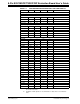
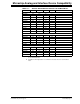
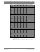
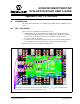
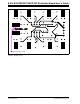
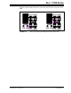
Figure D-3 shows how the pad can be connected to either the V
DD
or V
SS
plane of the
PCB.
FIGURE D-3: Alternate Jumpering the PCB pad to either VSS or VDD.
Jumpering to VSS
Jumpering to VDD