
User manual

8-Pin SOIC/MSOP/TSSOP/DIP Evaluation Board User’s Guide
DS51544A-page 12 © 2005 Microchip Technology Inc.
2.4 8-PIN SOIC/MSOP/TSSOP/DIP EVALUATION BOARD DESCRIPTION
The 8-Pin SOIC/MSOP/TSSOP/DIP Evaluation Board PCB is designed to be flexible
in the type of device evaluation that can be implemented.
The following sections describe each element of this evaluation board in further detail.
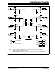
Refer to Figure 2-3.
2.4.1 Power and Ground
The 8-Pin SOIC/MSOP/TSSOP/DIP Evaluation Board has a VDD Pad and a VSS pad.
These pads can have connection posts installed that allows easy connection to the
power (V
DD
) and ground (V
SS
) planes. The layout allows either through-hole or
surface-mount connectors.
The power and ground planes are connected to the appropriate passive components
on the PCB (such as power plane to R2X and ground plane to R3X and C1X).
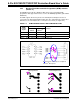
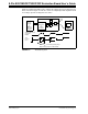
2.4.2 PCB PADs
For each package pin (pins 1 to 8), there is a PCB pad (pads 1 to 8). The device will
have some power pins (V
DD
) and some ground pins (V
SS
). To ease connections on the
PCB, vias to the power and ground plane have been installed close to each PCB pad.
This allows any pad to be connected to the power or ground plane, so when power is
connected to the VDD and VSS pads, the power is connected to the appropriate device
pin.
FIGURE 2-3: Jumpering the PCB pad to either VDD or VSS.
Revision 1 of this PCB has an issue that these vias are not connected to the desired
power and ground planes (they are open). For additional information, refer to
Appendix D. “Rev. 1 PCB Errata”.
Jumpering to VSS
Jumpering to VDD