
User manual

8-Pin SOIC/MSOP/TSSOP/DIP Evaluation Board User’s Guide
DS51544A-page 10 © 2005 Microchip Technology Inc.
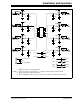
2.3.1 The Hardware
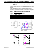
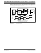
Figure 2-2 shows the layout of the 8-Pin SOIC/MSOP/TSSOP/DIP Evaluation Board.
This is a small four-layer board (1.5" x 2" (38.1 mm x 50.8 mm)). There are ten
connection points/pads that can use either through-hole or surface-mount connector
posts.
The pad labeled VDD is connected to the PCB power plane, while the pad labeled VSS
is connected to the PCB ground plane. All the passive components that are connected
to VDD or VSS are connected to either the power plane or ground plane.
The eight remaining PCB pads correspond to the device pins (i.e.; pad 1 connects to
pin 1).
Each pad has four passive components associated with them: a pull-up resistor, a
pull-down resistor, an in-line resistor and a filtering/load capacitor. The pull-up resistor
is always R2X, the pull-down resistor is R3X, the in-line resistor is R1X and the
filtering/load capacitor is C1X. The “X” is an alpha character that corresponds to a
particular pad (A to H). As an example, Pad 5’s pull-up resistor is R2E.
The green area of Figure 2-2 shows the silk-screen on the bottom layer of the PCB.
This is where the details of the implemented circuit can be written.
Capacitor C1 is the power supply filtering capacitor.
Capacitors C2 and C3 are bypass capacitors that may be required to be installed,
depending on the device selected and the system requirements (such as the noise
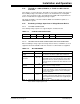
present on the power supply). Table 2-1 describes the components.
A 6-pin header interface is available that supports the PICmicro MCU Baseline Flash
Microcontroller Programmer (BFMP) interface. For additional information, refer to
Section 2.4.5 “Baseline Flash Microcontroller Programmer (BFMP) Interface
(Header J1)”.
FIGURE 2-2: 8-Pin SOIC/MSOP/TSSOP/DIP Evaluation Board Layout.